A kind of p-type crystalline silicon solar cell with transparent electrode and preparation method thereof
A technology for solar cells and transparent electrodes, applied in the field of solar cells, can solve the problems of rare application, poor matching, and high contact resistance, and achieve the effects of avoiding power loss, balancing the dilemma and reducing production costs.
- Summary
- Abstract
- Description
- Claims
- Application Information
AI Technical Summary
Problems solved by technology
Method used
Image


Examples
preparation example Construction
[0039] The method for preparing a P-type crystalline silicon backside partial contact solar cell with a transparent electrode is as follows:
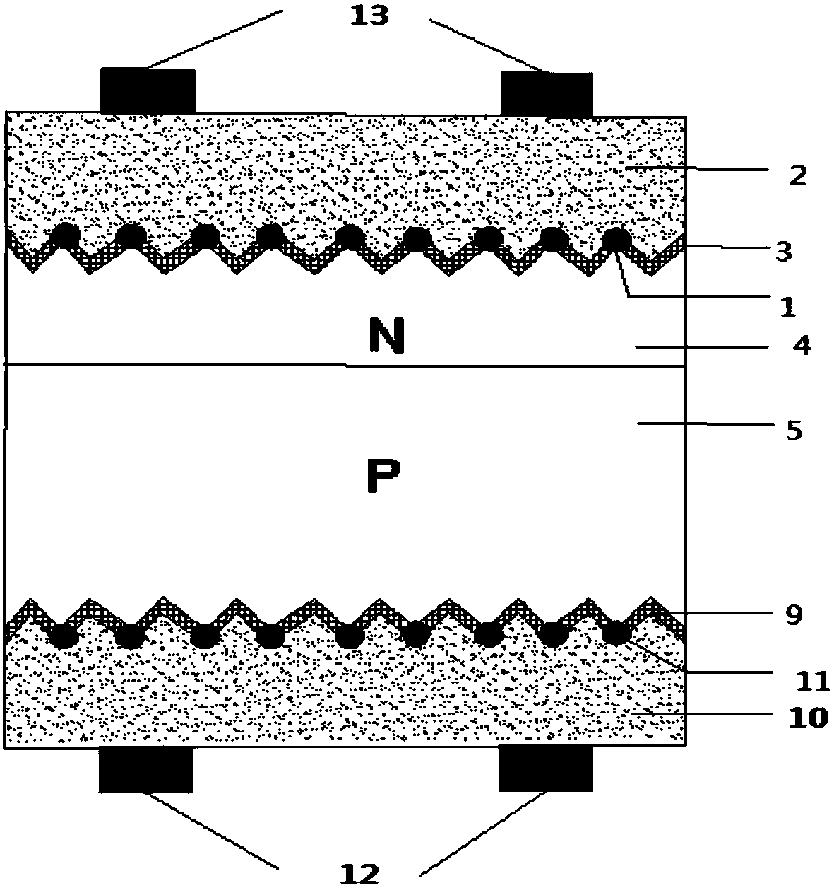
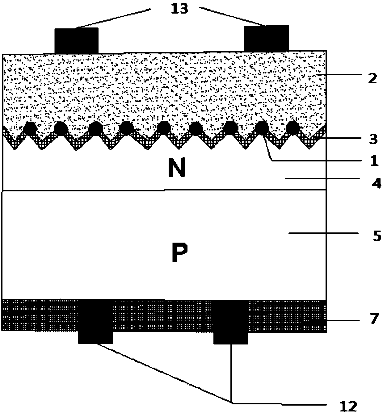
[0040] (1) Surface texture treatment of P-type crystalline silicon wafers. The silicon wafers can be P-type single crystal silicon wafers and polycrystalline silicon wafers. The texture treatment can be chemical liquid corrosion, plasma etching, metal catalysis, and laser etching. and other methods.
[0041] (2) Use the phosphorus source as an impurity to form a uniform impurity layer of 40-100Ω / □, and the phosphorus source can be POCl 3 、PH 3 , phosphorus slurry, etc. The method of making the impurity layer can be atmospheric pressure diffusion, low pressure diffusion, ion implantation, phosphorus-containing slurry coating, etc.
[0042] (3) Etching removes the dead layer and the back junction, and the etching method can be wet etching or dry etching.
[0043] (4) Deposit or grow a passivation film of 5-50nm and an anti-reflection f...
Embodiment 1
[0058] (1) Anisotropic etching of P-type monocrystalline silicon wafers in a KOH solution at around 80°C to obtain a surface pyramid structure;
[0059] (2) with POCl 3 As an impurity, diffuse at about 800°C to form a uniform diffusion layer of 80Ω / □;
[0060] (3) Remove the phosphosilicate glass and the back junction by wet etching;
[0061] (4) Deposit silicon oxide of about 5nm and silicon nitride of about 80nm on the front;
[0062] (5) Aluminum oxide of about 30nm and silicon nitride of about 80nm are deposited successively on the back;
[0063] (6) Print phosphorous-containing dopants and boron-containing dopants on the front and back according to specific patterns, the printed pattern adopts a dot array, the diameter of a single dot is 50um, and the distance between dots is 0.8mm;
[0064] (7) Use laser to pulse heat the dopant according to the specific pattern described in step (6), so that the phosphorus atoms on the front side and the boron atoms on the back side ...
Embodiment 2
[0067] (1) Forming an inverted pyramid structure on the surface of a P-type single crystal silicon wafer by catalytic chemical etching of nanometer metal particles;
[0068] (2) by pH 3 As impurities, a uniform diffusion layer of 90Ω / □ is formed by ion implantation;
[0069] (3) The dead layer and back junction are removed by wet etching;
[0070] (4) Deposit about 80nm silicon oxynitride on the front side
[0071] (5) Deposit aluminum oxide of about 30nm on the back;
[0072] (6) adopt laser to carry out hole to aluminum oxide film on the back, adopt the method for vapor deposition to prepare back electrode again, and carry out annealing treatment;
[0073](7) Spray phosphorus-containing dopants on the front according to a specific pattern, the spray pattern adopts a dot array, the diameter of a single point is 100um, and the distance between points is 1.5mm;
[0074] (8) Use a laser to pulse heat the dopant according to the specific pattern described in step (7), so that...
PUM
 Abstract
Description
Claims
Application Information
 - R&D
- Intellectual Property
- Life Sciences
- Materials
- Tech Scout
- Unparalleled Data Quality
- Higher Quality Content
- 60% Fewer Hallucinations
Browse by: Latest US Patents, China's latest patents, Technical Efficacy Thesaurus, Application Domain, Technology Topic, Popular Technical Reports.
© 2025 PatSnap. All rights reserved.Legal|Privacy policy|Modern Slavery Act Transparency Statement|Sitemap|About US| Contact US: help@patsnap.com