Fin-type field effect transistor forming method

一种鳍式场效应管、鳍部的技术,应用在电气元件、半导体/固态器件制造、电路等方向,能够解决应力层质量差、鳍式场效应管电学性能低下等问题,达到刻蚀损伤小、提高电学性能、高选择性的效果

Active Publication Date: 2016-06-29
SEMICON MFG INT (SHANGHAI) CORP
View PDF5 Cites 8 Cited by
  • Summary
  • Abstract
  • Description
  • Claims
  • Application Information

AI Technical Summary

Problems solved by technology

[0007] However, the quality of the stress layer formed by the prior art is poor, resulting in poor electrical performance of the FinFET

Method used


Image

  • Fin-type field effect transistor forming method
  • Fin-type field effect transistor forming method
  • Fin-type field effect transistor forming method

Examples


Embodiment Construction

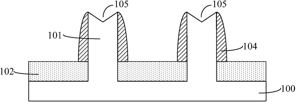
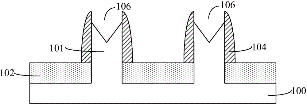
[0037] It can be seen from the background art that the quality of the stress layer formed in the prior art is poor, which leads to the low performance of the FinFET.

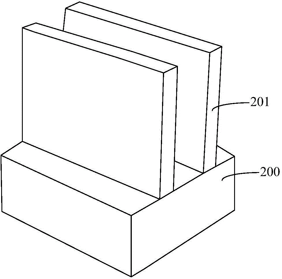
[0038] Please refer to figure 1, in one embodiment, a substrate 100 having fins 101 is provided, an isolation layer 102 is formed on the surface of the substrate 100 between adjacent fins 101, and the isolation layer 102 covers part of the sidewall surface of the fins 101 , and the top surface of the isolation layer 102 is lower than the top surface of the fin 101; a barrier layer covering the surface of the isolation layer 102, the sidewall and the top surface of the fin 101 is formed; a maskless etching process is used to etch and remove the The top surface of the fin portion 101 and the barrier layer on the surface of the isolation layer 102 form a sidewall layer 104 on the sidewall surface of the fin portion 101 , exposing the top surface of the fin portion 101 .

[0039] The function of the sidewall layer...


PUM


Abstract

The invention discloses a fin-type field effect transistor forming method, and the method comprises the steps: providing a substrate, wherein the surface is provided with a plurality of separated fin parts; forming a separation layer on the surface of the substrate, wherein the top of the separating layer is lower than the top of the fin parts, and covers the surface of a part of side walls of the fin parts; forming a side wall layer covering the surfaces of the side walls of the fin parts, and exposing the top surfaces of the fin parts; carrying out the selective nitrogen treatment of the tops of the fin parts, and enabling the fin parts at a certain thickness to be converted into a semiconductor nitridation layer; carrying out the etching of the semiconductor nitridation layer through employing a wet etching method, so as to form openings between the adjacent side wall layers and the remaining fin parts; and placing stress layers in the openings. The method improves the flatness of the bottom of the opening, improves the quality of the formed stress layers, and optimizes the electrical performances of a fin-type field effect transistor.

Description

technical field [0001] The invention relates to the technology in the field of semiconductor manufacturing, in particular to a method for forming a fin field effect transistor. Background technique [0002] With the continuous development of semiconductor process technology, the development trend of semiconductor process nodes following Moore's Law continues to decrease. In order to adapt to the reduction of process nodes, the channel length of MOSFET field effect transistors has to be continuously shortened. The shortening of the channel length has the advantages of increasing the die density of the chip and increasing the switching speed of the MOSFET field effect tube. [0003] However, as the channel length of the device is shortened, the distance between the source and the drain of the device is also shortened, so that the control ability of the gate to the channel becomes worse, and the gate voltage pinches off (pinchoff) the channel. The difficulty is also increasin...

Claims


Application Information

Patent Timeline
Patent Type & Authority Applications(China)
IPC IPC(8): H01L21/336
CPCH01L29/7848H01L29/165H01L21/02252H01L29/66795H01L29/785H01L21/0217H01L21/02247
Inventor 何永根吴兵
Owner SEMICON MFG INT (SHANGHAI) CORP
Why Eureka
Try Eureka