Photosensitive conductive film, conductive pattern formation method using same, and conductive pattern substrate
A conductive pattern and conductive film technology, which is applied in the formation of conductive patterns and the field of conductive pattern substrates, can solve the problems of reduced yield, long process, and high cost burden, and achieve low contact resistance, sufficient adhesion, and good electrical connection Effect
- Summary
- Abstract
- Description
- Claims
- Application Information
AI Technical Summary
Problems solved by technology
Method used
Image
Examples
Embodiment 1
[0181]
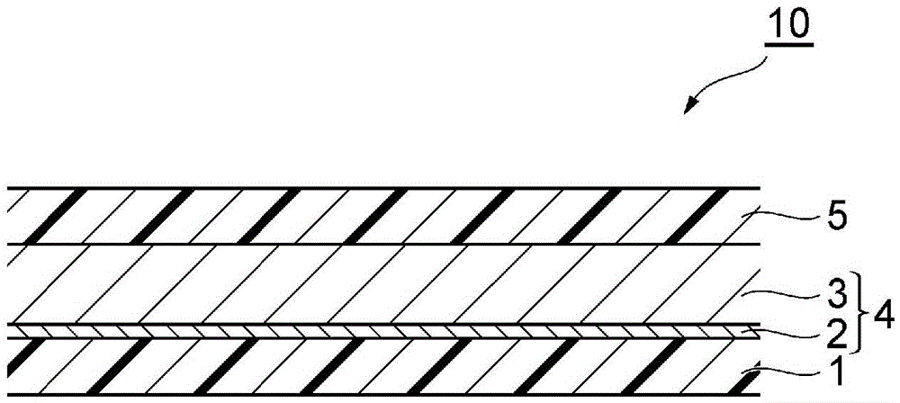
[0182] On a polyethylene terephthalate film (PET film, manufactured by Teijin Co., Ltd., trade name: G2-16) with a thickness of 16 μm prepared as the first film (coating film) at 20 g / m 2 The above-mentioned conductive fiber dispersion liquid 1 was uniformly applied, dried by a hot air convection dryer at 100°C for 10 minutes, and pressed at room temperature (25°C) with a linear pressure of 1 MPa, thereby forming a layer containing Conductive layer of conductive fibers. In addition, as a result of measurement with a scanning electron micrograph, the film thickness after drying of the conductive layer was about 0.1 μm.
[0183] Then, on a polyethylene terephthalate film (PET film, manufactured by Teijin Co., Ltd., trade name: G2-50) with a thickness of 50 μm prepared separately as the second film (support film), it was evenly coated The solution (X) of the said photosensitive resin composition was dried for 10 minutes with the hot-air convection dryer of 100 degreeC...
Embodiment 2~10、 comparative example 1、2
[0210] A photosensitive resin composition was produced in the same manner as in Example 1 except that the solution (X) of the photosensitive resin composition obtained by compounding the materials shown in Table 2 was used in the compounding amounts (unit: parts by mass) shown in Table 2. For the conductive film, the surface resistivity, light transmittance, and electrical connectivity with the connection terminals on the surface of the substrate were evaluated for the conductive pattern. The results are shown in Table 2.
[0211] For each material in Table 2, the following materials were used.
[0212] (B) Ingredients
[0213] PET-30: Pentaerythritol triacrylate (manufactured by Nippon Kayaku Co., Ltd.)
[0214] TMPTA: Trimethylolpropane triacrylate (manufactured by Nippon Kayaku Co., Ltd.)
[0215] (C) Ingredients
[0216] OXE-01: 1,2-octanedione, 1-[4-(phenylthio)phenyl-2-(O-benzoyl oxime)] (manufactured by BASF Corporation)
[0217] (D) Ingredients
[0218] Silica fi...
Embodiment 11~13
[0230] The solution (X) of the photosensitive resin composition obtained by compounding the materials shown in Table 3 according to the compounding amount (unit: mass part) shown in Table 3 was used, and a photosensitive resin composition was produced in the same manner as in Example 1. For the conductive film, the surface resistivity, light transmittance, and electrical connectivity with the connection terminals on the surface of the substrate were evaluated for the conductive pattern. The results are shown in Table 3.
[0231] For each material in Table 3, the following materials were used.
[0232] (A) Ingredients
[0233] Acrylic polymer A: an acrylic resin having a copolymerization ratio of methacrylic acid / methyl methacrylate / ethyl acrylate / styrene=20 / 50 / 20 / 10, and a weight average molecular weight of 80,000
[0234] Acrylic polymer B: an acrylic resin having a copolymerization ratio of methacrylic acid / methyl methacrylate / ethyl acrylate / 2-hydroxyethyl methacrylate=20 / ...
PUM
| Property | Measurement | Unit |
|---|---|---|
| visible light transmittance | aaaaa | aaaaa |
| particle diameter | aaaaa | aaaaa |
| particle diameter | aaaaa | aaaaa |
Abstract
Description
Claims
Application Information
 - Generate Ideas
- Intellectual Property
- Life Sciences
- Materials
- Tech Scout
- Unparalleled Data Quality
- Higher Quality Content
- 60% Fewer Hallucinations
Browse by: Latest US Patents, China's latest patents, Technical Efficacy Thesaurus, Application Domain, Technology Topic, Popular Technical Reports.
© 2025 PatSnap. All rights reserved.Legal|Privacy policy|Modern Slavery Act Transparency Statement|Sitemap|About US| Contact US: help@patsnap.com


