Method of adopting two-dimensional graphene thin film to improve conductivity of substrate during electron beam nano gate writing
A graphene film and electron beam technology, applied in the field of microelectronics, can solve the problems of poor electrical conductivity and charge accumulation on the surface of the substrate, and achieve the effect of solving the phenomenon of slippage, good adhesion, and easy removal
- Summary
- Abstract
- Description
- Claims
- Application Information
AI Technical Summary
Problems solved by technology
Method used
Image

Examples
preparation example Construction
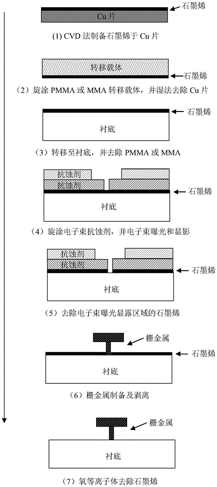
[0037] 8) preparing and stripping the gate metal;
[0038] 9) Removal of remaining graphene with oxygen plasma.
[0039] Wherein, the substrate prepared by the CVD method in step 1) of graphene is any one or more combinations of Cu, Ni, Ti, Ag, Al, Cr, Pd, Au, Mo, W, Fe. The material of the substrate can be selected according to needs, and is not strictly limited.
[0040] Preferably, the corrosion solution described in step (2) is any one of ferric chloride, ammonium persulfate, hydrogen chloride, sulfuric acid, nitric acid, hydrofluoric acid, aqua regia or a mixture thereof.
[0041] The target substrate described in step 4) includes Si, GaN, SiC, Al 2 o 3 , GaAs, SiO 2 , AlN, HfO 2 , Y 2 o 3 Any one or more of epitaxy and bonding assembly. The material of the target substrate can be selected according to needs, and is not strictly limited.
[0042] In step 5), the organic solution includes any one or a combination of acetone, NMP, and ethanol.
[0043] In step 6),...
Embodiment 1
[0048] A method for improving the conductivity of a substrate in electron beam nanogrid writing by using a two-dimensional graphene film, the specific process steps are as follows:
[0049] 1) Graphene is prepared on the metal Cu substrate by CVD method, and the PMMA transfer carrier is spin-coated on the graphene, and the thickness of the carrier is 100-300nm;
[0050] 2) The sample is placed in the corrosion solution with the PMMA transfer carrier facing up and the metal Cu facing down, the metal Cu below is dissolved, and the graphene is attached to the upper layer of PMMA;
[0051] 3) The sample is transferred to deionized water to wash away the residual ions carried out in the corrosion solution;
[0052] 4) Transfer the sample to the target substrate, such as common substrates such as gallium nitride, gallium arsenide, silicon carbide, and AlN;
[0053] 5) Soak in acetone to remove PMMA on the surface of the substrate, then soak in NMP (N-methylpyrrolidone) for 15 minut...
Embodiment 2
[0061] A method for improving the conductivity of a substrate in electron beam nanogrid writing by using a two-dimensional graphene film, the specific process steps are as follows:
[0062] 1) Graphene is prepared on the metal Cu substrate by CVD method, and the PMMA transfer carrier is spin-coated on the graphene, and the thickness of the carrier is 100-300nm;
[0063] 2) The sample is placed in the corrosion solution with the PMMA transfer carrier facing up and the metal Cu facing down, the metal Cu below is dissolved, and the graphene is attached to the upper layer of PMMA;
[0064] 3) The sample is transferred to deionized water to wash away the residual ions carried out in the corrosion solution;
[0065] 4) transferring the sample to a gallium arsenide substrate;
[0066] 5) Soak in acetone to remove PMMA on the surface of the substrate, then soak in NMP for 15 minutes, then pass through acetone and ethanol in turn, and finally wash with deionized water;
[0067] 6) Sp...
PUM
 Abstract
Description
Claims
Application Information
 - R&D
- Intellectual Property
- Life Sciences
- Materials
- Tech Scout
- Unparalleled Data Quality
- Higher Quality Content
- 60% Fewer Hallucinations
Browse by: Latest US Patents, China's latest patents, Technical Efficacy Thesaurus, Application Domain, Technology Topic, Popular Technical Reports.
© 2025 PatSnap. All rights reserved.Legal|Privacy policy|Modern Slavery Act Transparency Statement|Sitemap|About US| Contact US: help@patsnap.com