Method of forming semiconductor device

A semiconductor and device technology, applied in the field of semiconductor device formation, can solve the problems of dielectric layer dishing, affecting the reliability of semiconductor devices, etc., and achieve the effect of avoiding dishing

Active Publication Date: 2018-11-16
SEMICON MFG INT (SHANGHAI) CORP
View PDF5 Cites 0 Cited by
  • Summary
  • Abstract
  • Description
  • Claims
  • Application Information

AI Technical Summary

Problems solved by technology

[0003] In a specific process, when planarizing the dielectric layer and other hard materials at the same time, it will be found that dishing is easy to occur in the dielectric layer, such as grinding the dielectric layer and embedding in the dielectric layer at the same time. In the case of the gate structure of the NMOS transistor, since a metal interconnection structure will be fabricated on the above gate structure to lead out the signal of the NMOS transistor, at this time, if there is a dish-shaped depression in the dielectric layer, and the above-mentioned dish-shaped depression is filled with After adding conductive materials such as metal, it will affect the reliability of semiconductor devices

Method used


Image

  • Method of forming semiconductor device
  • Method of forming semiconductor device
  • Method of forming semiconductor device

Examples


Embodiment Construction

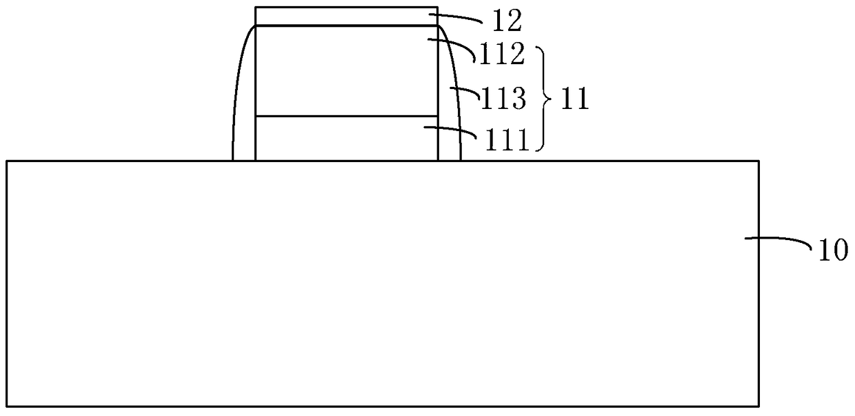
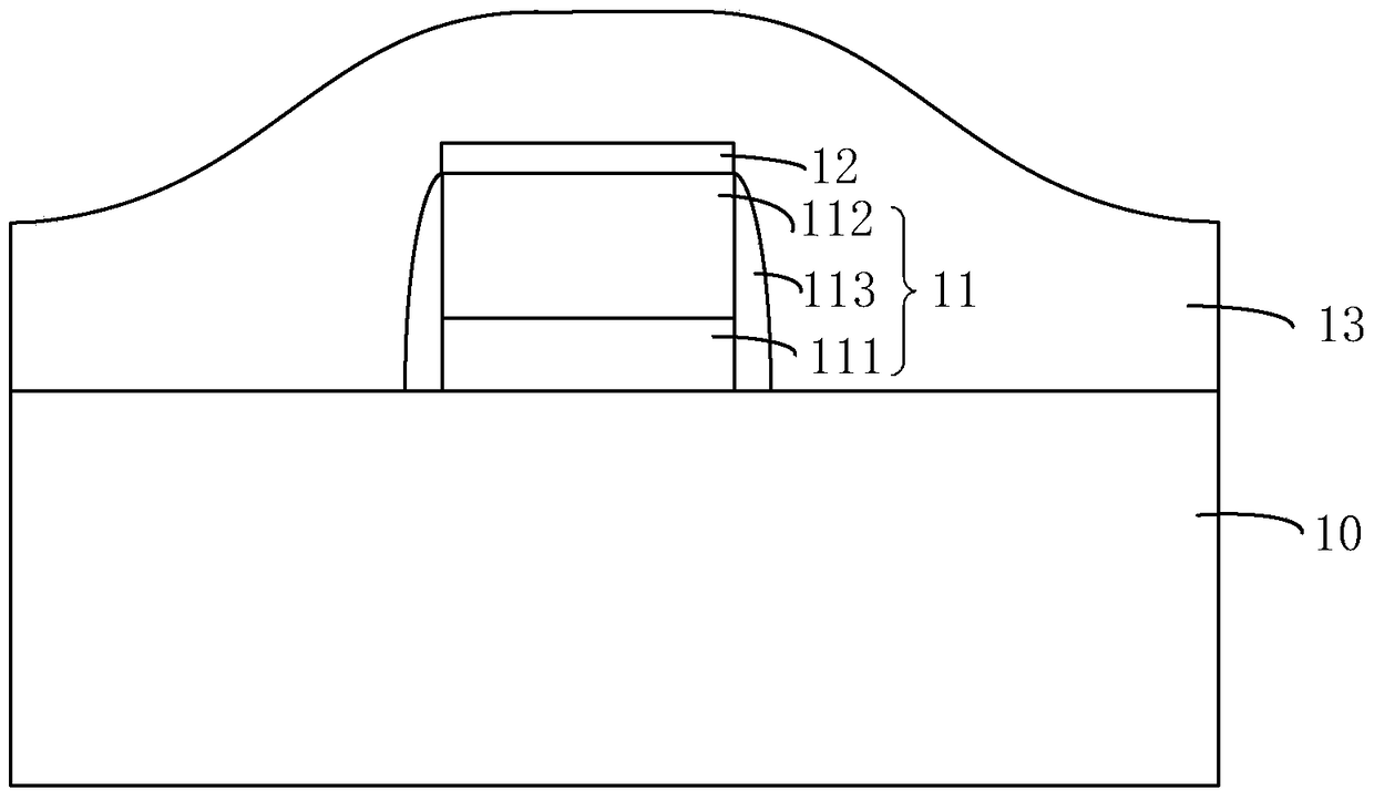
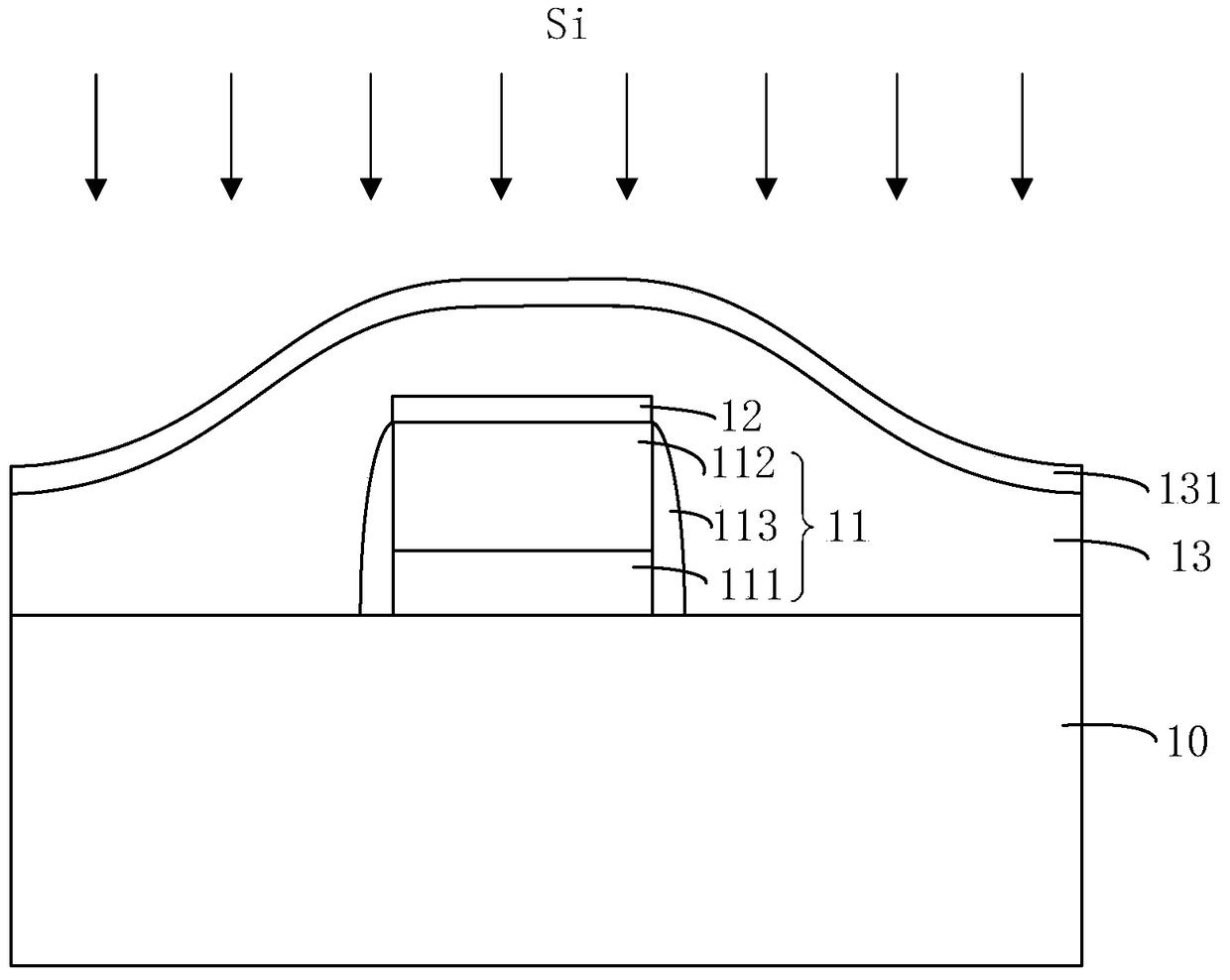
[0030] As mentioned in the background art, in the prior art, when the dielectric layer and surrounding hard materials are simultaneously ground, dish-shaped depressions are prone to appear in the dielectric layer. If the above-mentioned dish-shaped depressions are filled with conductive materials, it will affect the semiconductor device reliability. In view of the above technical problems, the present invention proposes to form a first dielectric layer and a second dielectric layer on a semiconductor substrate having a gate structure and an active region in two stages, wherein, after the formation of the first dielectric layer is completed, Implant silicon ions in it to form a silicon-doped layer, and then form a second dielectric layer on the silicon-doped layer; then grind the second dielectric layer and the first dielectric layer in two stages, the first stage is based on the gate structure The silicon-doped layer on the top is the grinding end point. For the second dielect...


PUM


Abstract

The invention relates to a formation method of a semiconductor device. A first dielectric layer and a second dielectric layer are formed on a semiconductor substrate having a gate structure and an active region at two stages, wherein silicon ion injection is carried out after completion of formation of the first dielectric layer to form a silicon doping layer, and then the second dielectric layer is formed on the silicon doping layer. And the second dielectric layer and the first dielectric layer are ground at two stages until the top surface of the gate structure is exposed; at the first stage, the silicon doping layer at the top of the gate structure is used as a grinding end point, and the second dielectric layer arranged on the silicon doping layer is removed by using a rapid grinding way, so that the grinding efficiency becomes high; and at the second stage, grinding is carried out until the top surface of the gate structure is reached, and the first dielectric layer arranged under the silicon doping layer is processed by a slow grinding way. Therefore, equal grinding on the first dielectric layer at the top of the gate structure and the second dielectric layer and the first electric layer at the surrounding area can be realized, thereby avoiding a dish-shaped depression at the surface of the dielectric layer.

Description

technical field [0001] The invention relates to the technical field of semiconductors, in particular to a method for forming a semiconductor device. Background technique [0002] In the manufacturing process of semiconductor devices, the chemical mechanical polishing (CMP) process is a common planarization technology used to reduce the surface height difference of semiconductor structures, which utilizes the mechanical grinding and chemical corrosion of the polishing liquid . [0003] In a specific process, when planarizing the dielectric layer and other hard materials at the same time, it will be found that dishing is easy to occur in the dielectric layer, such as grinding the dielectric layer and embedding in the dielectric layer at the same time. In the case of the gate structure of the NMOS transistor, since a metal interconnection structure will be fabricated on the above gate structure to lead out the signal of the NMOS transistor, at this time, if there is a dish-sha...

Claims


Application Information

Patent Timeline
Patent Type & Authority Patents(China)
IPC IPC(8): H01L21/336H01L21/3105
Inventor 梁海慧周祖源
Owner SEMICON MFG INT (SHANGHAI) CORP
Why Eureka
Try Eureka