
Superimposition marker and method for producing the same

A manufacturing method and marking technology, which are used in semiconductor/solid-state device manufacturing, electrical components, electrical solid-state devices, etc., can solve problems such as defects in the active region, collapse of overlapping marks, etc., so as to avoid problems where the overlapping error value cannot be measured. Effect

Active Publication Date: 2010-07-07
WINBOND ELECTRONICS CORP
View PDF5 Cites 0 Cited by
  • Summary
  • Abstract
  • Description
  • Claims
  • Application Information

AI Technical Summary

Problems solved by technology

Although this method does not affect the alignment measurement due to the dishing phenomenon of the isolation structure, due to the lateral etching phenomenon that usually occurs in the subsequent step of removing the conductor layer by wet etching, the photoresist The conductive layer under the pattern is removed causing the overlay mark to collapse, thus causing defect problems in the active area

Method used


Image

  • Superimposition marker and method for producing the same
  • Superimposition marker and method for producing the same
  • Superimposition marker and method for producing the same

Examples


Embodiment Construction

[0038] To make the above-mentioned features and advantages of the present invention more comprehensible, the following specific embodiments are described in detail with reference to the accompanying drawings.

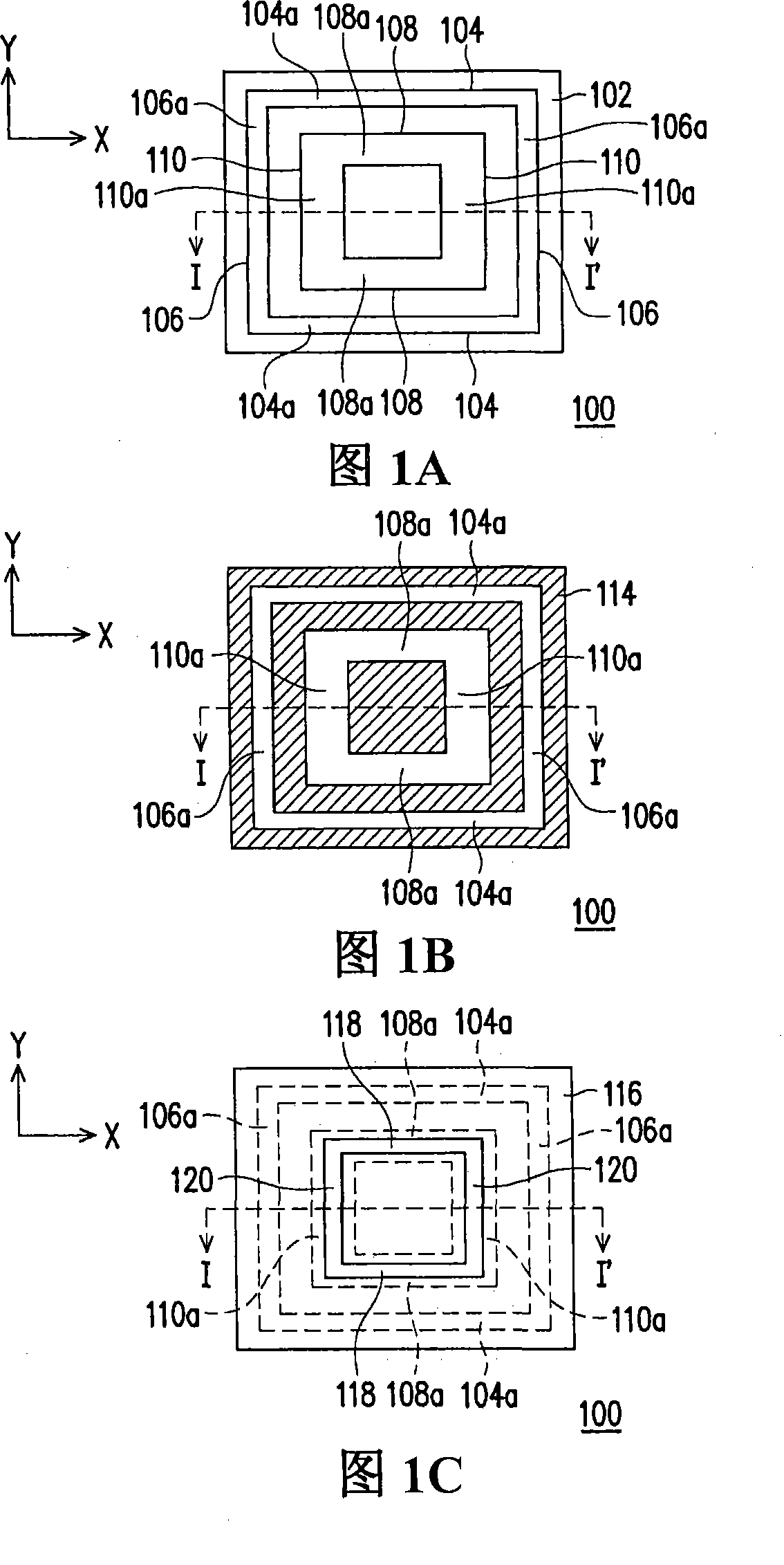
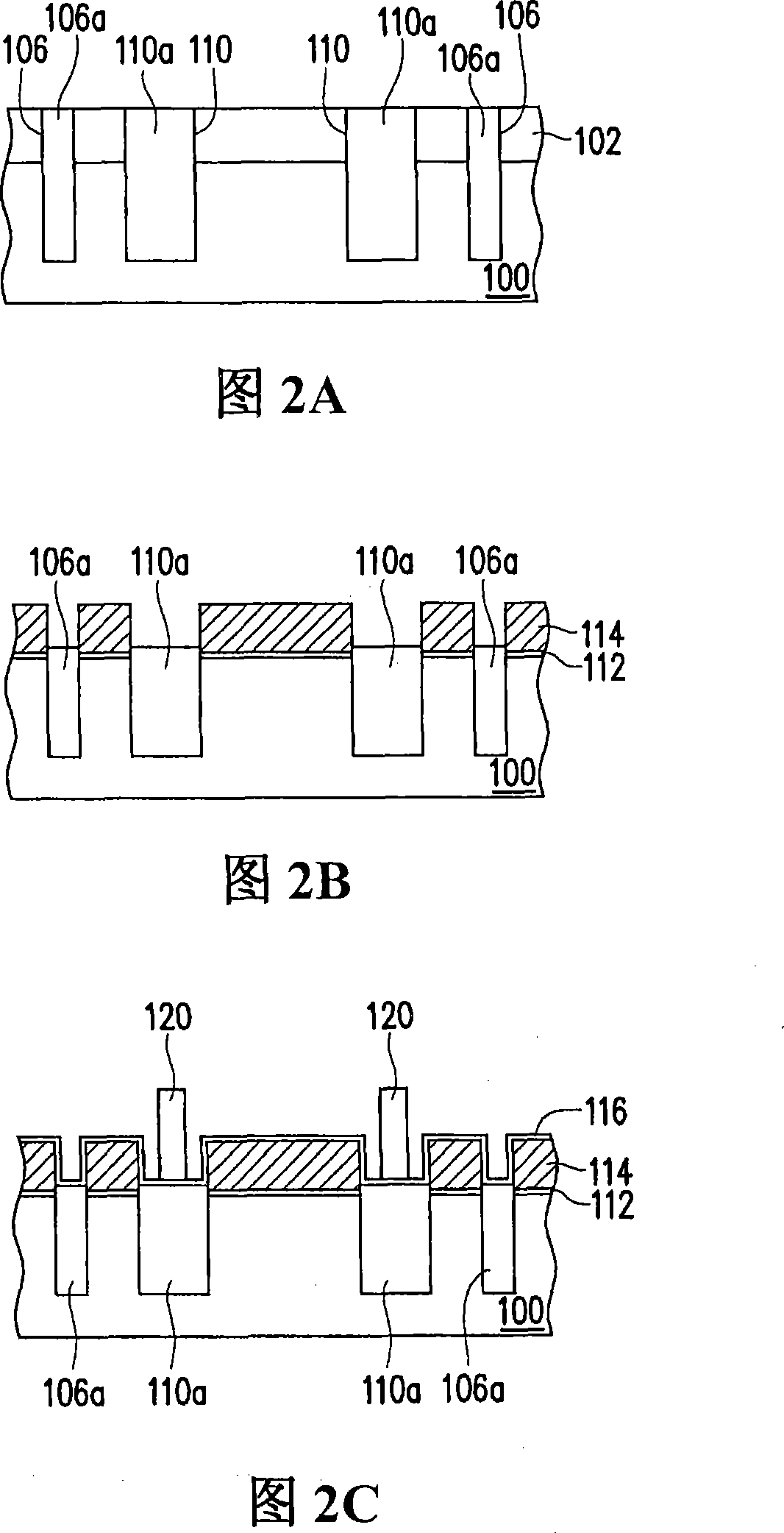
[0039] Figure 1A to Figure 1C It is a top view of the manufacturing process of the superposition mark according to the embodiment of the present invention. Figure 2A to Figure 2C According to Figure 1A to Figure 1C The cross-sectional view of the production process of the superimposed marker shown in the I-I section in . In particular, in the following description of the present invention, the film layers used to form the overlay mark in the peripheral area are all in the same process step as the film layers used to form the non-volatile memory in the component area. formed in.

[0040] First, referring to FIG. 1A and FIG. 2A simultaneously, a hard mask layer 102 is formed on the substrate 100 in the peripheral area. The substrate 100 is, for example, a silicon su...


PUM


Abstract

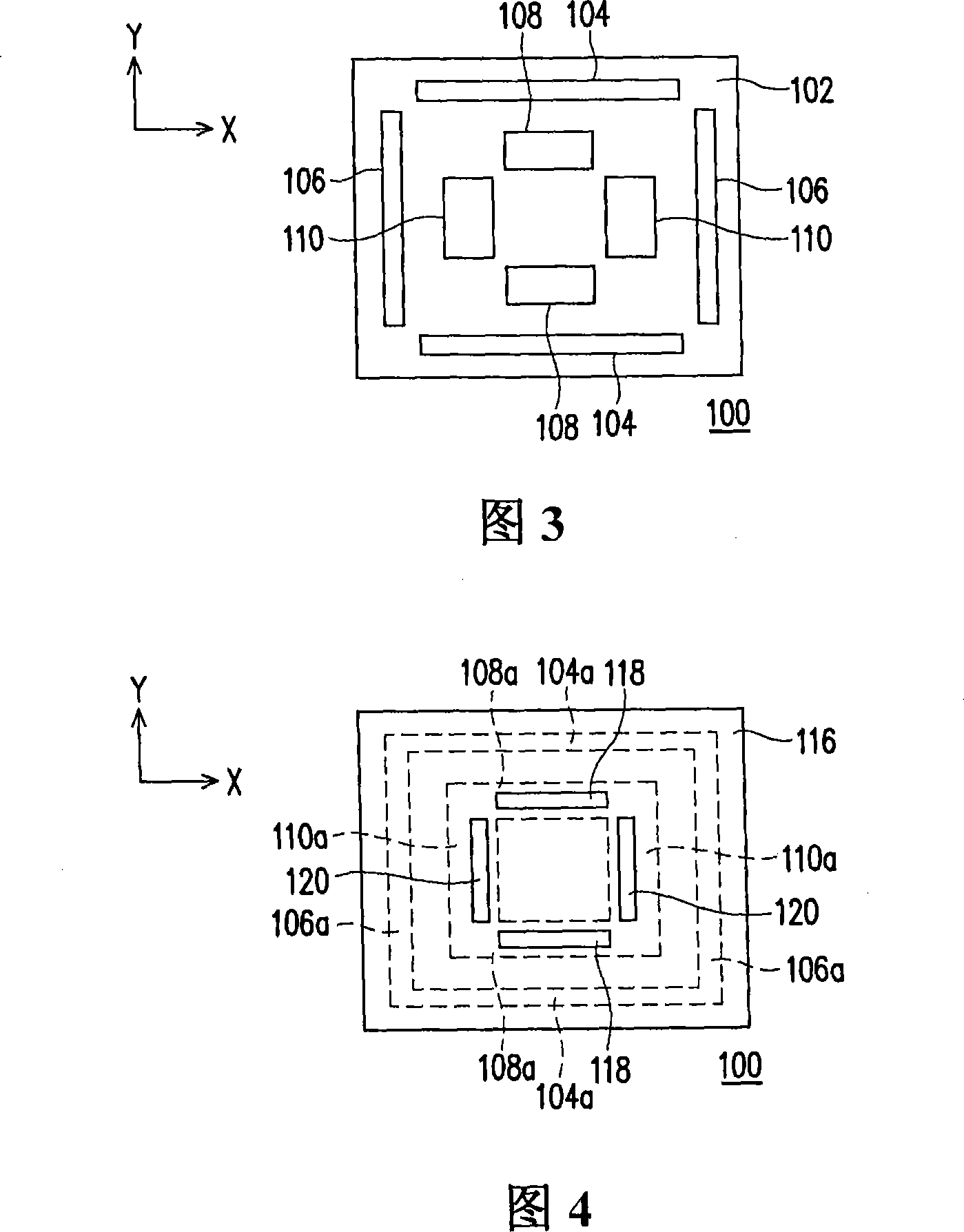
The invention provides a superimposition marker and a production method thereof. The method comprises the steps that two first X-direction isolation structures, two first Y-direction isolation structures, two second X-direction isolation structures and two second Y-direction isolation structures are formed in a substrate, wherein, the first X-direction isolation structures and the first Y-direction isolation structures are arranged to form a first rectangle; and the second X-direction isolation structures and the second Y-direction isolation structures are arranged to form a second rectangle which is arranged in the first rectangle. A first dielectric layer and a conductor layer are formed on the substrate in sequence. A planarization technology is carried out to remove partial conductor layer until the isolation structures are exposed. A second dielectric layer is formed on the substrate and a rectangular pattern is formed on the second dielectric layer, and sides of the rectangular pattern are respectively positioned above the isolation structures.

Description

technical field [0001] The present invention relates to a superposition mark and its manufacturing method, and in particular to a superposition mark and its manufacturing method which can avoid affecting alignment measurement results and preventing defects. Background technique [0002] Under the circumstances that the integration degree of the semiconductor process is gradually increasing, the complexity and difficulty of the process steps are also getting higher and higher. Therefore, how to use real-time measurement equipment to monitor the process and respond to problems in real time to reduce losses caused by process errors has become the direction of efforts of various semiconductor process manufacturers. [0003] As the line width of the integrated circuit process continues to shrink, apart from critical dimension (CD) control, another important factor that determines the success or failure of the wafer photolithography process is alignment accuracy. Therefore, the m...

Claims


Application Information

Patent Timeline
Patent Type & Authority Patents(China)
IPC IPC(8): H01L21/00H01L23/544
Inventor 陈敏鸿蔡高财
Owner WINBOND ELECTRONICS CORP
Learn More