
Gallium-antimonide-based semiconductor device provided with interface passivation layer and preparation method thereof

A gallium antimonide-based, passivation layer technology, applied in the fields of semiconductor/solid-state device manufacturing, semiconductor devices, electrical components, etc., can solve the problems of low interface quality and poor device performance, and achieve reduced defect density and interface state density. Reduce and improve the effect of media quality

Inactive Publication Date: 2015-06-17
SOUTHEAST UNIV
View PDF4 Cites 5 Cited by
  • Summary
  • Abstract
  • Description
  • Claims
  • Application Information

AI Technical Summary

Problems solved by technology

However, the interface quality is not high and the device performance is poor

Method used


Image

  • Gallium-antimonide-based semiconductor device provided with interface passivation layer and preparation method thereof
  • Gallium-antimonide-based semiconductor device provided with interface passivation layer and preparation method thereof
  • Gallium-antimonide-based semiconductor device provided with interface passivation layer and preparation method thereof

Examples


preparation example Construction

[0038]A method for preparing a gallium antimonide-based semiconductor device with an interface passivation layer based on claim 1, comprising the following steps:

[0039] Step 1, cleaning the gallium antimonide substrate surface to remove surface contamination and natural oxide layer;

[0040] Step 2, selectively implanting ions in the surface area of ​​the substrate, annealing and activating, forming a second conductivity type impurity implantation layer, and evaporating source and drain contact metals in the corresponding areas;

[0041] Step 3, deposit the gate dielectric, and immediately transfer it to the plasma chamber for plasma bath treatment to form an interface passivation layer;

[0042] Step 4, evaporating the gate metal and performing subsequent processes of the semiconductor device.

[0043] In the first step, the gallium antimonide substrate cleaning includes organic solution cleaning and / or pickling.

[0044] In the second step, the implanted ions are Si, Mg...

example

[0053] A schematic diagram of a typical preparation process flow of a GaSb-based semiconductor device with an interface passivation layer, as shown in Figure 2, wherein:

[0054] Figure 2A It is a gallium antimonide substrate (201) after organic cleaning and pickling. For organic cleaning, use acetone and ethanol to wash alternately several times, and then rinse repeatedly with deionized water to remove oil and organic pollutants on the substrate; then pickle with a hydrochloric acid solution with a concentration of 1% to 36% by mass Soak for 1-10 minutes, then rinse with deionized water repeatedly, and blow dry with nitrogen to remove the natural oxide layer. The purpose of cleaning is to remove organic and inorganic pollutants, metal particles, natural oxide layer, etc. on the substrate, but it is not limited to the above cleaning methods.

[0055] Figure 2B Al 2 o 3 , SiO 2 or Si 3 N 4 Ions are implanted into the GaSb substrate (201) of the protective layer (202)....


PUM


Abstract

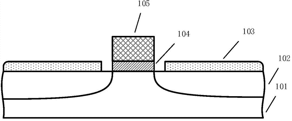
The invention discloses a gallium-antimonide-based semiconductor device provided with an interface passivation layer and a preparation method thereof. The gallium-antimonide-based semiconductor device provided with the interface passivation layer comprises a first conductive type impurity gallium antimonide substrate (101), a second conductive type impurity injection layer (102), a source electrode and drain electrode layer (103), a passivated gate medium (104) and a grid electrode (105) which are sequentially arranged from bottom to top. When the gallium-antimonide-based semiconductor device is prepared, an interface of the gallium antimonide semiconductor device is passivated by introducing plasma containing the fluorine element, and therefore a plurality of fluorine passivation interface layers are formed. Stable metal-fluorine keys are formed through fluorine passivation treatment, and volume defects in the gate medium and gate medium / gallium antimonide interface traps are obviously reduced. The metal-fluorine keys are reflected onto the gallium-antimonide-based semiconductor device, so gate leakage and interface-state density are reduced, and the stability and electrical properties of the device are further greatly improved.

Description

technical field [0001] The invention relates to a gallium antimonide-based semiconductor device with an interface passivation layer and a preparation method thereof, belonging to the technical field of semiconductor devices Background technique [0002] As device dimensions are scaled closer and closer to the limit of silicon, III–V compound semiconductors are beginning to gain traction as channel materials for metal-oxide-semiconductor field-effect transistors (MOSFETs). Gallium antimonide (GaSb) has the highest hole mobility (~1400cm 2 / Vs), at the same time, the band gap of GaSb is 0.73eV, which can effectively maintain the switching ratio of the surface channel transistor, and because the Fermi level of GaSb is pinned to the valence band, the p-type GaSb can Forming low-resistivity ohmic contacts with metals, these conditions are favorable for the preparation of GaSb-based pMOSFETs. [0003] Since gallium antimonide is easily oxidized when exposed to air, GaO is formed...

Claims


Application Information

Patent Timeline
Patent Type & Authority Applications(China)
IPC IPC(8): H01L29/78H01L21/336
CPCH01L29/78H01L29/20H01L29/30H01L29/42364H01L29/66477
Inventor 张雄曾振华崔一平刘凯
Owner SOUTHEAST UNIV
Learn More