
Preparation method of conductive organic matter/silicon nanowire solar cell and product thereof

A technology of conductive organic matter and solar cells, applied in the field of solar cells, can solve problems such as large surface area, affecting cell efficiency, and inability to effectively control the diameter of nanowires, so as to achieve high efficiency and improve cell efficiency

Inactive Publication Date: 2015-05-06
ZHEJIANG UNIV
View PDF7 Cites 9 Cited by
  • Summary
  • Abstract
  • Description
  • Claims
  • Application Information

AI Technical Summary

Problems solved by technology

Although silicon nanowires prepared by traditional methods can effectively reduce the reflectivity, due to the large surface area, there is a serious problem of carrier recombination, which reduces the minority carrier lifetime of silicon nanowires, thereby affecting the efficiency of the cell [Zhang, J.; Zhang, Y.; Zhang, F.; Sun, B. Electrical characterization of inorganic-organic hybrid photovoltaic devices based on silicon-poly(3,4-ethylenedioxythiophene):poly(styrenesulfonate).Appl.Phys.Lett.2013,102,013501 .]
At the same time, the silicon nanowires prepared by traditional methods are disordered and disordered, and the diameter of the nanowires cannot be effectively controlled, and the minority carrier lifetime of the silicon nanowires cannot be controlled.

Method used


Image

  • Preparation method of conductive organic matter/silicon nanowire solar cell and product thereof
  • Preparation method of conductive organic matter/silicon nanowire solar cell and product thereof
  • Preparation method of conductive organic matter/silicon nanowire solar cell and product thereof

Examples


Embodiment 1

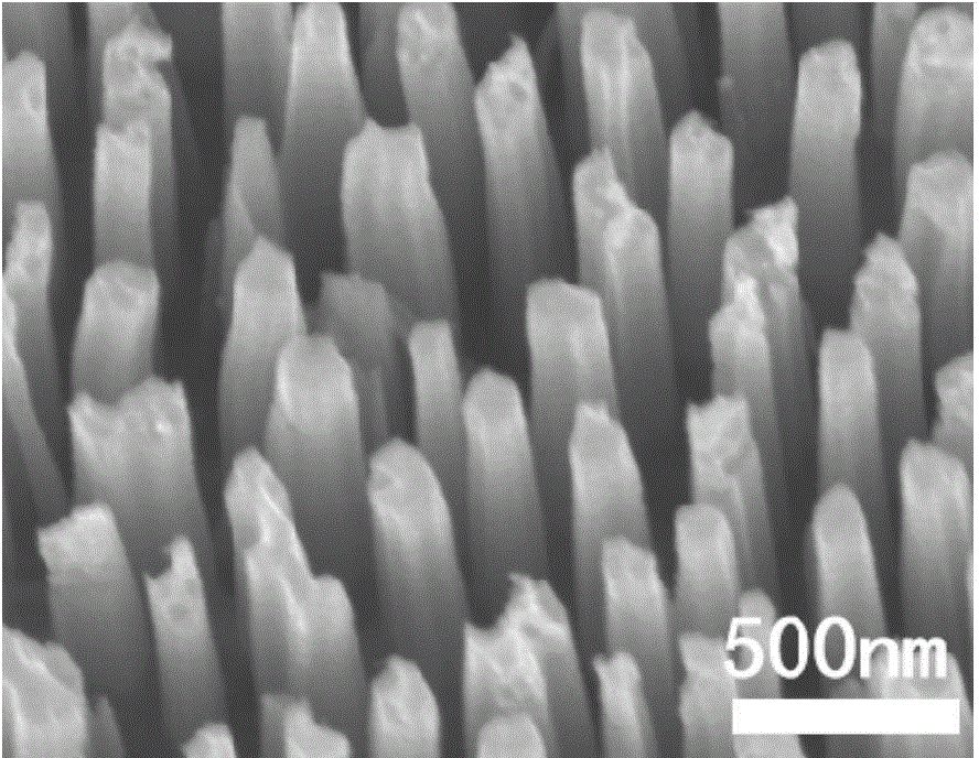
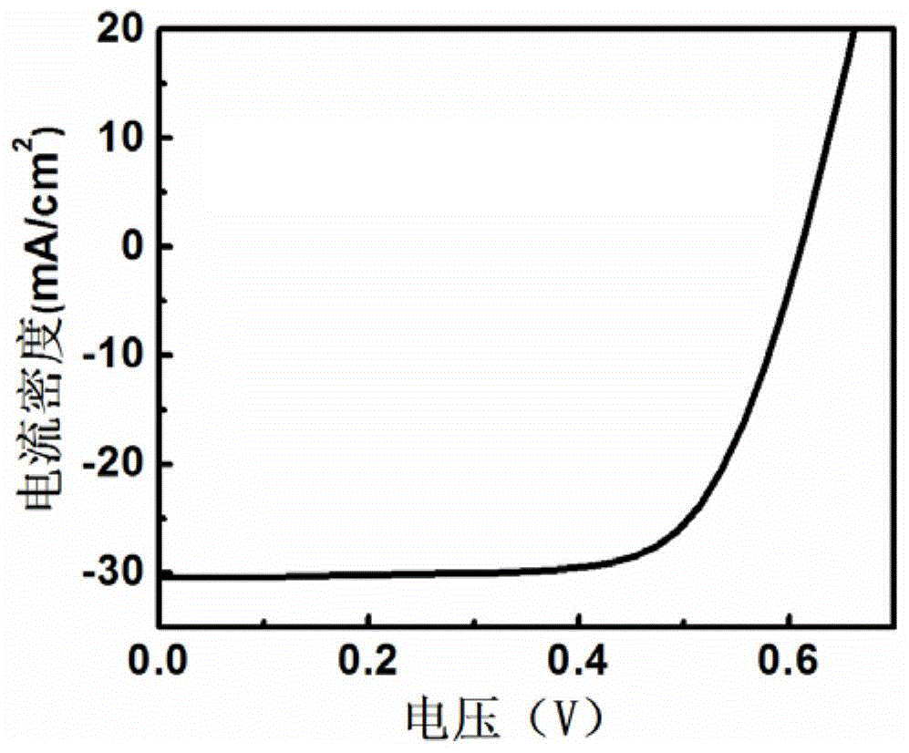
[0035] Sputter gold on the aluminum oxide template for 90s, then transfer the gold film to a silicon wafer, place it in a mixed solution of hydrofluoric acid (40% by mass) and hydrogen peroxide (30% by mass) and etch to obtain silicon Nanowires. Under an oxygen atmosphere, at 1000°C, after thermal oxidation for 360 minutes, silicon oxide is formed on the surface of the silicon nanowire, and then soaked in a hydrofluoric acid solution with a mass fraction of 30% until the silicon oxide is completely removed, and the treated silicon nanowire is obtained. The diameter is 90 ~ 100nm. Soak the treated silicon nanowires in an aqueous solution of 0.5% tetramethylammonium hydroxide for 60s; spin-coat PEDOT doped with dimethyl sulfoxide and polyethylene glycol octylphenyl ether on the surface :PSS, dimethyl sulfoxide, PEDOT: The mass ratio of PSS to polyethylene glycol octyl phenyl ether is 7:92:1, the spin coating speed is 2000r / min, heat treatment is carried out at 100 °C, and the h...

Embodiment 2

[0038]Sputter gold on the aluminum oxide template for 90s, then transfer the gold film to a silicon wafer, place it in a mixed solution of hydrofluoric acid (40% by mass) and hydrogen peroxide (30% by mass) and etch to obtain silicon Nanowires. In an oxygen atmosphere, at 900°C, after thermal oxidation treatment for 600 minutes, silicon oxide was generated on the surface of the silicon nanowires, and then soaked in a hydrofluoric acid solution with a mass fraction of 5% until the silicon oxide was completely removed, and the treated silicon nanowires were obtained. The diameter of the root is 65-75nm. Soak the treated silicon nanowires in an aqueous solution of 1% tetramethylammonium hydroxide for 90s; spin-coat silicon nanowires doped with dimethyl sulfoxide and polyethylene glycol octylphenyl The PEDOT:PSS of ether, the mass ratio of dimethyl sulfoxide, PEDOT:PSS and polyethylene glycol octyl phenyl ether is 5:94:1, spin-coating speed is 3000r / min, and carry out heat treatm...

Embodiment 3

[0041] Sputter gold on the aluminum oxide template for 90s, then transfer the gold film to a silicon wafer, place it in a mixed solution of hydrofluoric acid (40% by mass) and hydrogen peroxide (30% by mass) and etch to obtain silicon Nanowires. In an oxygen atmosphere, at 800°C, after thermal oxidation for 700 minutes, silicon oxide is formed on the surface of the silicon nanowire, and then soaked in a hydrofluoric acid solution with a mass fraction of 30% until the silicon oxide is completely removed, and the treated silicon nanowire is obtained. The diameter is 35 ~ 40nm. Soak the treated silicon nanowires in an aqueous solution with a mass fraction of 1.5% tetramethylammonium hydroxide for 120s; spin-coat silicon nanowires doped with dimethyl sulfoxide and polyethylene glycol octylphenyl The PEDOT:PSS of ether, the mass ratio of dimethylsulfoxide, PEDOT:PSS and polyethylene glycol octyl phenyl ether is 9:90:1, and spin-coating speed is 5000r / min, and heat treatment is car...


PUM

PropertyMeasurementUnit
Diameteraaaaaaaaaa
Short circuit current densityaaaaaaaaaa
Diameteraaaaaaaaaa

Abstract

The invention discloses a preparation method of a conductive organic matter / silicon nanowire solar cell. The preparation method includes the steps of: taking aluminum oxide as a template, and combining with a metal-assisted chemical etching method to prepare silicon nanowires, thermally oxidizing for 60-800min at the temperature of 800-1000 DEG C to generate silicon oxide on the surfaces of the silicon nanowires, and steeping into hydrofluoric acid solution until the silicon oxide is completely removed; steeping the processed silicon nanowires into tetramethylammonium hydroxide solution, rotationally coating conductive organic matters on the surfaces after taking out of the solution, and further thermally processing to obtain knotted silicon nanowires; then respectively depositing silver and aluminum on the fronts and backs of the knotted silicon nanowires to serve as electrodes, and thereby obtaining the conductive organic matter / silicon nanowire solar cell. The invention provides a preparation method of the conductive organic matter / silicon nanowire solar cell; according to the preparation method, the silicon nanowires with ordered arrangement and controllable diameter can be prepared, and thereby the conductive organic matter / silicon nanowire solar cell with significantly improved cell efficiency can be prepared.

Description

technical field [0001] The invention relates to the technical field of solar cells, in particular to a method for preparing a conductive organic matter / silicon nanowire solar cell and its products. Background technique [0002] In today's world, non-renewable energy sources such as coal and oil are frequently in emergency, and the energy crisis has restricted economic development. At the same time, the abnormal global climate and deteriorating environmental problems caused by conventional energy sources have also attracted much attention. More and more countries are turning their attention to renewable energy, and the development of solar energy resources has become a global trend. Solar cells have three advantages of permanence, cleanliness and flexibility. In the solar cell industry, solar cells based on crystalline silicon account for more than 80%, but compared with conventional energy sources, the total market share is still very small. This is mainly because cost iss...

Claims


Application Information

Patent Timeline
IPC IPC(8): H01L51/48H01L51/46
CPCH10K85/40H10K30/00Y02E10/549
Inventor 余学功沈鑫磊杨德仁
Owner ZHEJIANG UNIV
Learn More