Method for Integrating Power Devices and Control Devices

A technology for controlling devices and integrating power, which is applied in semiconductor/solid-state device manufacturing, electric solid-state devices, semiconductor devices, etc. It can solve the problem of poor compatibility between power devices and control devices, affecting device performance optimization, and occupying a large area and other issues to achieve the effect of reducing aspect ratio, reducing difficulty and improving performance

Active Publication Date: 2017-08-04
WUHAN XINXIN SEMICON MFG CO LTD
View PDF5 Cites 0 Cited by
  • Summary
  • Abstract
  • Description
  • Claims
  • Application Information

AI Technical Summary

Problems solved by technology

However, this solution needs to place the source region of the device on the back of the silicon wafer, which is inconsistent with the conventional vertical power device where the source region of the device is placed on the front of the silicon wafer, so the existing vertical power devices cannot be applied to this solution.
And multiple chips are spread out and connected on the plane, occupying a large area
[0006] The single-chip solution is to integrate the power device and the control device in the same chip through special chip design and production. The entire process is the sum of the processes of the two devices. The device has undergone unnecessary processes and the cost is high.
Moreover, the performance compatibility of power devices and control devices is not strong, which affects the optimization of the performance of both devices

Method used


Image

  • Method for Integrating Power Devices and Control Devices
  • Method for Integrating Power Devices and Control Devices
  • Method for Integrating Power Devices and Control Devices

Examples


Embodiment Construction

[0060] The present invention will be further described below in conjunction with the accompanying drawings and specific embodiments, but not as a limitation of the present invention.

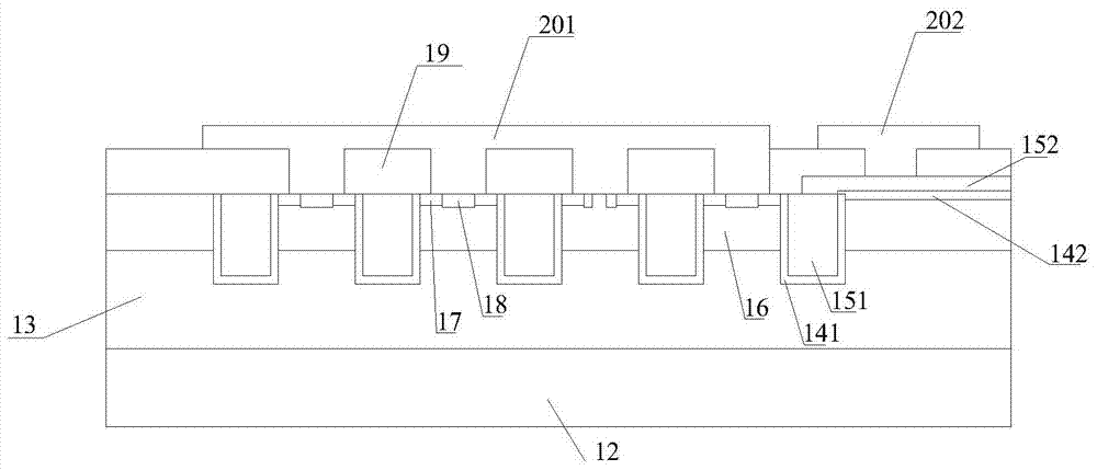
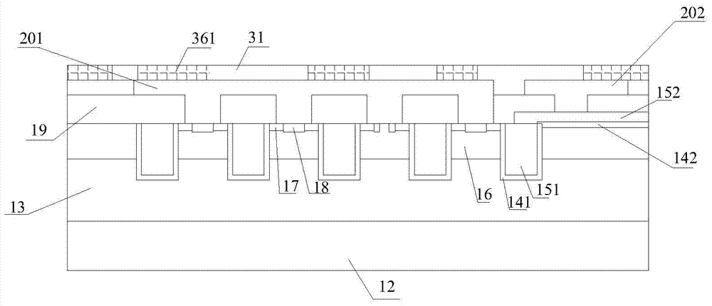
[0061] like Figure 14 As shown, the present invention provides a method for integrating power devices and control devices, comprising the following steps:

[0062] Provide a power chip prepared with a power device and a control chip prepared with a control device, and the power chip is provided with a drain region; the power device has a source electrode and a gate electrode, and the control device has a first control electrode and a second control electrode. electrode;

[0063] A first dielectric layer is deposited on the front of the power chip and the front of the control device, and part of the first dielectric layer is respectively etched to form a plurality of first openings, a plurality of second openings, a plurality of first openings and the plurality of first openings. The above-men...


PUM


Abstract

The present invention relates to the technical field of integrated circuit manufacturing, and in particular to an integration method of a power device and a control device. Through the method of the present invention, the power chip and the control chip can be designed and manufactured independently of each other, ensuring their performance and cost advantages At the same time, the interconnection of the control circuit and the chip device can be completed without using wiring and conventional packaging; and by sharing the thinning and back metal process, the manufacturing cost is further reduced, and the performance of the power device is improved at the same time, and due to the thickened The metal on the back drain of the power device further reduces the on-resistance of the device. In addition, the use of metal rewiring improves the heat dissipation performance, and stops on the metal layer of the power chip through silicon vias, reducing the through-silicon vias. The aspect ratio reduces the difficulty of process realization.

Description

technical field [0001] The invention relates to the technical field of semiconductor manufacturing, in particular to a method for integrating power devices and control devices. Background technique [0002] Field Effect Transistors (FETs) are widely used in various electronic circuits. It is a voltage-controlled semiconductor device. It has the advantages of high input resistance (107~1015Ω), low noise, low power consumption, large dynamic range, easy integration, no secondary breakdown phenomenon, and wide safe working area. It has become a powerful bipolar transistor and power transistor. competitor. The manufacturing process of the control device of the field effect tube is completely different from that of the field effect tube. However, the work of the field effect tube depends on the connection of the control device. Therefore, obtaining the field effect transistor and its control device at the same time has become a technical difficulty in this field. [0003] At ...

Claims


Application Information

Patent Timeline
Patent Type & Authority Patents(China)
IPC IPC(8): H01L21/60H01L21/98
CPCH01L24/02H01L24/03H01L25/50
Inventor 肖胜安程卫华梅绍宁鞠韶复朱继锋
Owner WUHAN XINXIN SEMICON MFG CO LTD
Why Eureka
Try Eureka