A high-power infrared light-emitting diode
An infrared light-emitting and diode technology, which is applied in the direction of electrical components, circuits, semiconductor devices, etc., can solve the problems of peeling off of oxides and metal mirrors and epitaxial layers, poor thermal conductivity of oxide materials, and poor heat dissipation performance of chips
- Summary
- Abstract
- Description
- Claims
- Application Information
AI Technical Summary
Problems solved by technology
Method used
Image
Examples
Embodiment 1
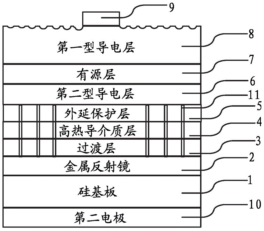
[0059] Such as figure 1 As shown, a high-power infrared light-emitting diode disclosed by the present invention includes a silicon substrate 1, a metal reflector 2, a transition layer 3, a high thermal conductivity medium layer 4, an epitaxial protective layer 5, and an epitaxial light-emitting structure; the epitaxial light-emitting structure includes an active Layer 7, first-type conductive layer 8 and second-type conductive layer 6.
[0060] A first-type conductive layer 8 is arranged on one side of the active layer 7, a first electrode 9 is arranged on the first-type conductive layer 8, a second-type conductive layer 6 is arranged on the other side, and an epitaxial protective layer 5 is arranged on the second-type conductive layer 6 .
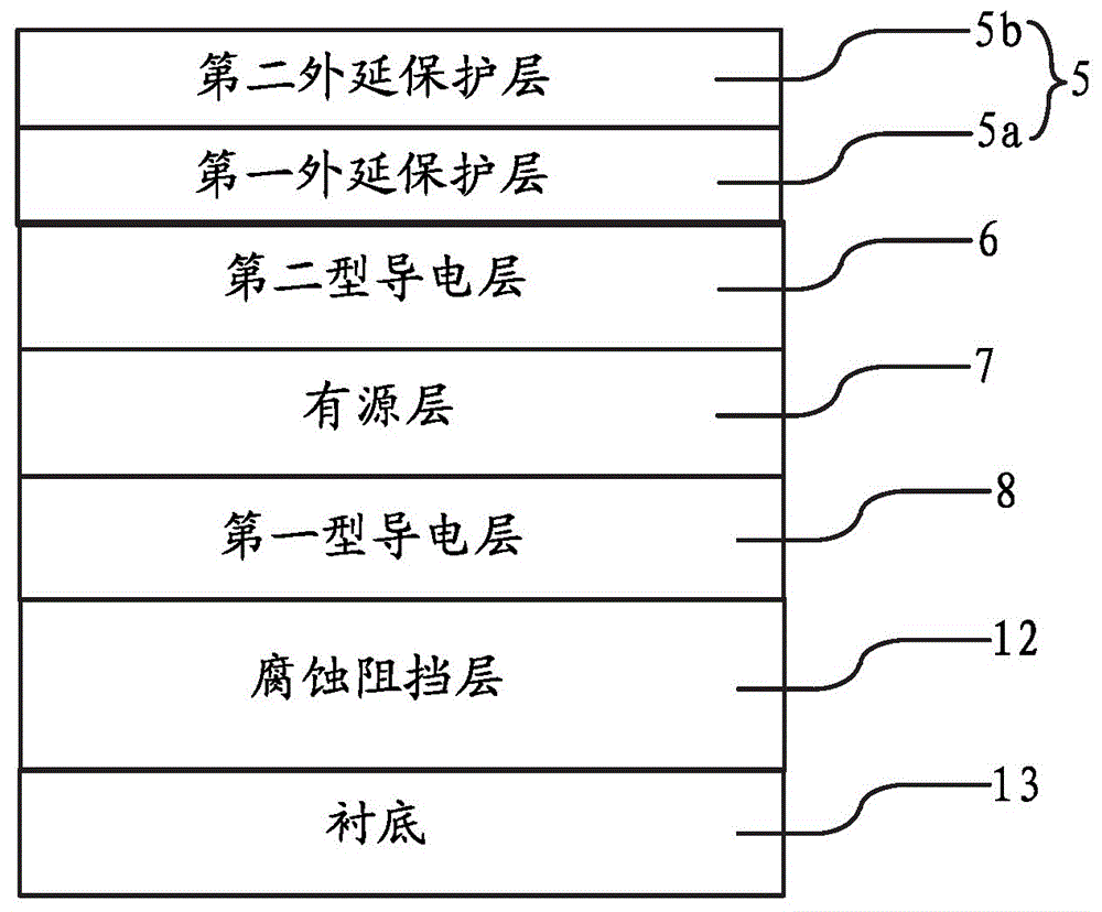
[0061] Such as figure 2 As shown, the epitaxial protective layer 5 is composed of a first epitaxial protective layer 5a and a second epitaxial protective layer 5b, the first epitaxial protective layer 5a is in contact with the second-ty...
Embodiment 2
[0081] The difference from Embodiment 1 is: a method for manufacturing a high-power infrared light-emitting diode, comprising the following steps:
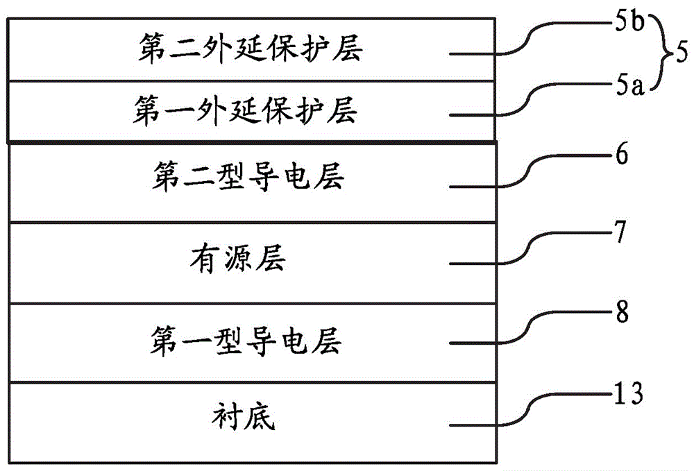
[0082] one, such as image 3 In the shown epitaxial structure, on the surface of the substrate 13 from bottom to top, there are first type conductive layer 8 , active layer 7 , second type conductive layer 6 , and epitaxial protective layer 5 . The epitaxial protection layer 5 is composed of two parts, a first epitaxial protection layer 5a and a second epitaxial protection layer 5b. Compared with the first embodiment, the epitaxial structure is not provided with the corrosion barrier layer 12 .
[0083] The substrate 13 is a GaAs substrate. The first-type conductive layer 8 is made of AlGaInP group III-V compound material, and has a thickness of 9 μm. The active layer 7 adopts a quantum well structure composed of AlGaInAs and AlGaAs two materials alternately, the logarithm of alternate composition is 10 pairs, and the light emi...
PUM
 Abstract
Description
Claims
Application Information
 - R&D Engineer
- R&D Manager
- IP Professional
- Industry Leading Data Capabilities
- Powerful AI technology
- Patent DNA Extraction
Browse by: Latest US Patents, China's latest patents, Technical Efficacy Thesaurus, Application Domain, Technology Topic, Popular Technical Reports.
© 2024 PatSnap. All rights reserved.Legal|Privacy policy|Modern Slavery Act Transparency Statement|Sitemap|About US| Contact US: help@patsnap.com


