A flexible high-light-trapping radial-junction heterojunction high-efficiency crystalline silicon solar cell and its preparation method
A solar cell and heterojunction technology, applied in photovoltaic power generation, circuits, electrical components, etc., can solve the problems of conversion efficiency, open-circuit voltage drop, short-circuit current density reduction, and technical route difficulty, so as to improve conversion efficiency and conversion efficiency. The effect of high and low recombination probability
- Summary
- Abstract
- Description
- Claims
- Application Information
AI Technical Summary
Problems solved by technology
Method used
Image
Examples
Embodiment 1
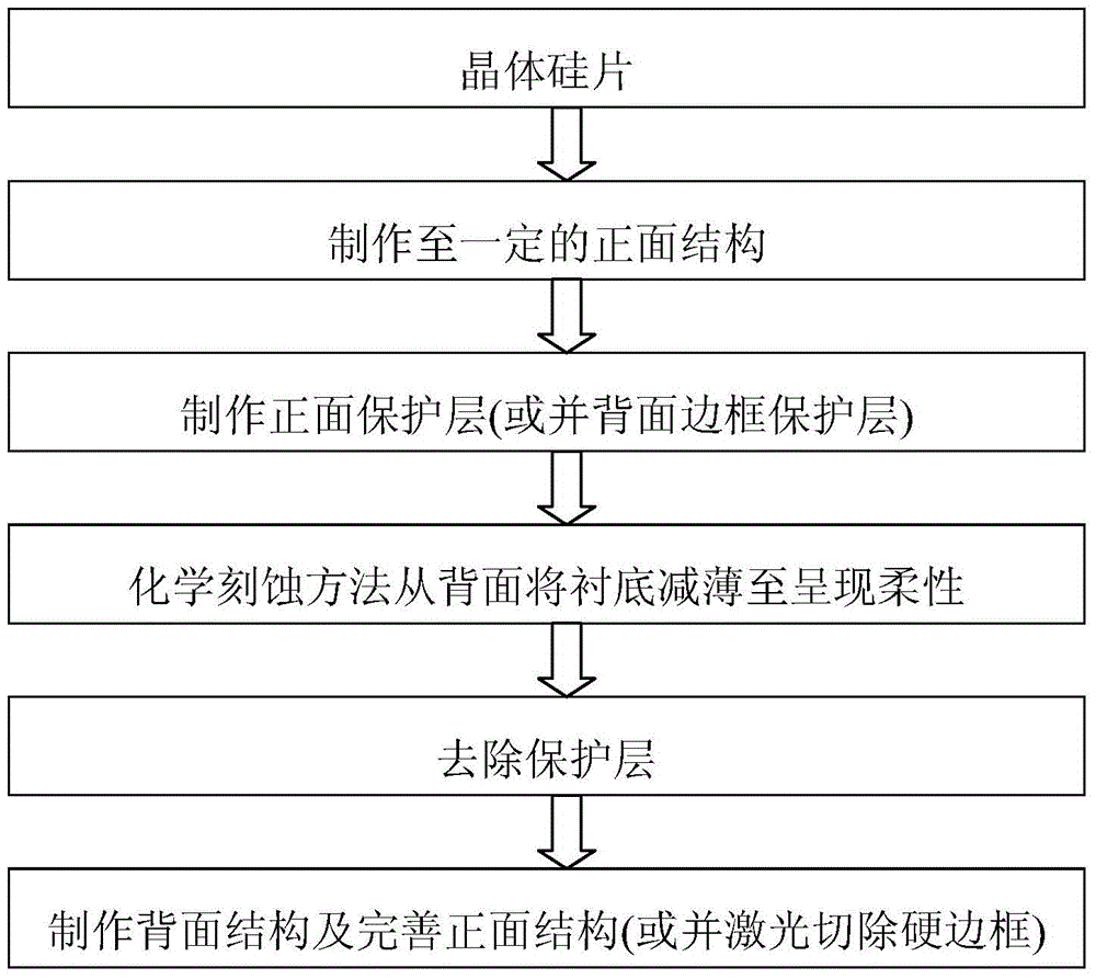
[0025] Example 1, the front side is fabricated to form a columnar array structure with high light trapping property, and the front side is protected by etching the back side:
[0026] 1) A p-type monocrystalline silicon wafer with a thickness of 200±20um and a resistivity of 1-3Ω·cm is used as the substrate.
[0027] 2) Perform conventional alkali texturing on the substrate.
[0028] 3) Using contact ultraviolet lithography to form a circular array of holes on the front photoresist; vapor-deposit metal chromium of 0.1-10um on it, and form a circular array of chromium by stripping the photoresist; use metal chromium The circular array is a mask plate, which is etched by fluorine-based RIE to form a columnar array of crystalline silicon; the surface damage of metal chromium and silicon is removed by chemical wet method; A crystalline silicon columnar array structure with a height of 3-10um.
[0029] 4) PECVD deposits 300-600nm SiNx on the front side as a protective layer, and ...
Embodiment 2
[0038] Example 2, the front is fabricated until the TCO / metal electrode is deposited, the front is protected and the back is etched:
[0039] 1) An n-type monocrystalline silicon wafer with a thickness of 200±20um and a resistivity of 50-500Ω·cm is used as the substrate.
[0040] 2) Perform conventional chemical polishing on the substrate.
[0041] 3) Using contact ultraviolet lithography to form a circular array on the front photoresist; electron beam evaporation of 5-500nm metal silver on it, and forming a silver circular hole-shaped array by stripping the photoresist; The metal silver in the circular hole array is used as a catalytic aid, and chemical wet etching is performed to form a columnar array of crystalline silicon; the surface damage of metallic silver and silicon is removed by chemical wet method; finally, a diameter of 2-20um and a period of 4- 40um, crystalline silicon columnar array structure with a height of 3-10um.
[0042] 4) The front PECVD first deposits...
PUM
 Abstract
Description
Claims
Application Information
 - R&D
- Intellectual Property
- Life Sciences
- Materials
- Tech Scout
- Unparalleled Data Quality
- Higher Quality Content
- 60% Fewer Hallucinations
Browse by: Latest US Patents, China's latest patents, Technical Efficacy Thesaurus, Application Domain, Technology Topic, Popular Technical Reports.
© 2025 PatSnap. All rights reserved.Legal|Privacy policy|Modern Slavery Act Transparency Statement|Sitemap|About US| Contact US: help@patsnap.com


