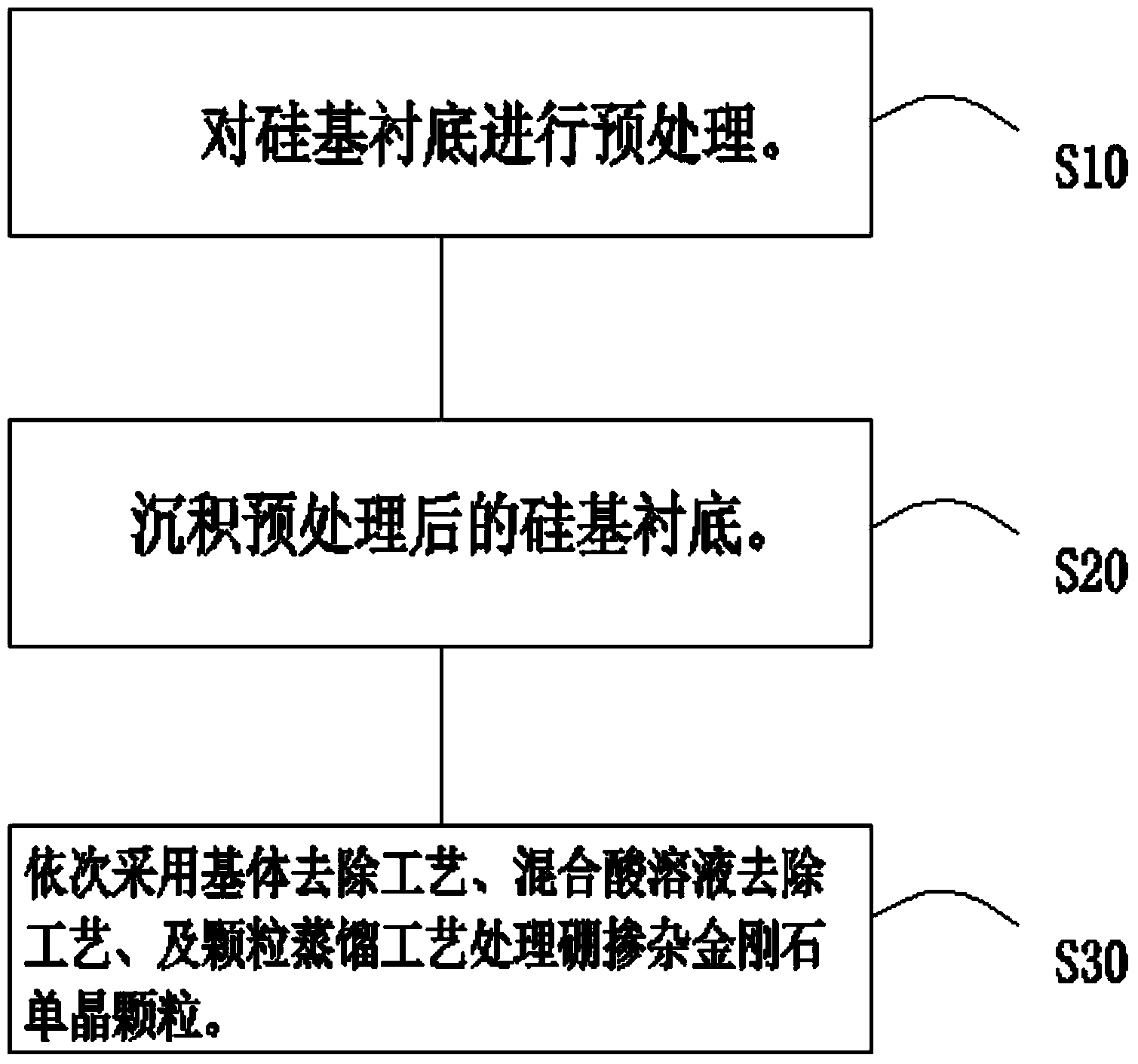
Preparation method of boron-doped ultra/fine diamond monocrystal micropowder
A diamond single crystal, boron-doped technology, applied in the field of diamond manufacturing, can solve the problems of difficulty in single crystal purification, unsuitable for high-efficiency synthesis of boron-doped single crystal diamond powder, etc., to achieve improved crystal shape and surface quality, high impact resistance , The effect of simple process
- Summary
- Abstract
- Description
- Claims
- Application Information
AI Technical Summary
Problems solved by technology
Method used
Image
Examples
Embodiment 1
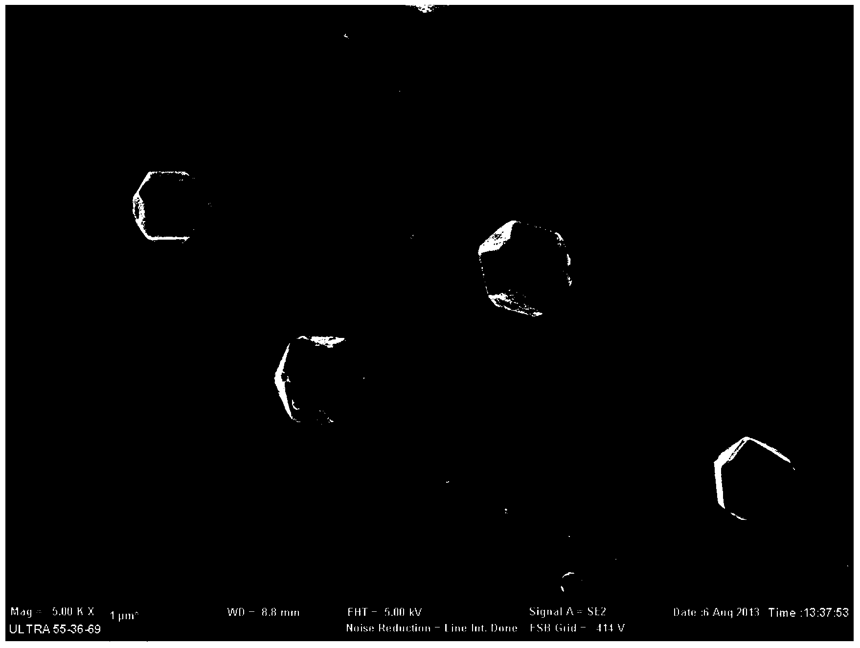
[0035] The CVD high-grade super / fine diamond single-crystal micropowder with an average particle size of 1.8 μm is prepared on a mirror-polished single-crystal silicon wafer.
[0036] First, the surface of the silicon-based substrate was uniformly mechanically ground for 0.5 min with 0.5 μm diamond micropowder, and then the mechanically ground silicon-based substrate was ultrasonically cleaned in deionized water and acetone solution for 3 min.
[0037] Next, put the pretreated silicon-based substrate into the reaction chamber of the hot-wire CVD device for deposition. The hot-wire adopts a twisted-pair tantalum wire with a diameter of Φ0.4mm, and arranges the hot-wire in parallel on the silicon-based substrate. Above, and use high temperature resistant springs to keep the hot wire in a straight and horizontal state during the deposition process. After the reaction chamber is evacuated, the reaction gas (hydrogen and acetone) is introduced, wherein the acetone is brought into t...
Embodiment 2
[0041] The CVD high-grade super / fine diamond single-crystal micropowder with an average grain size of 2.4 μm is prepared on a mirror-polished single-crystal silicon wafer.
[0042] First, the silicon-based substrate surface was uniformly mechanically ground for 1 min with 2 μm diamond micropowder, and then the mechanically ground silicon-based substrate was ultrasonically cleaned in deionized water and acetone solution for 5 min.
[0043] Next, put the pretreated silicon-based substrate into the reaction chamber of the hot-wire CVD device for deposition. The hot-wire adopts a twisted-pair tantalum wire with a diameter of Φ0.4mm, and arranges the hot-wire in parallel on the silicon-based substrate. Above, and use high temperature resistant springs to keep the hot wire in a straight and horizontal state during the deposition process. After the reaction chamber is evacuated, the reaction gas (hydrogen and acetone) is introduced, wherein the acetone is brought into the reaction ch...
Embodiment 3
[0047] The CVD high-grade super / fine diamond single-crystal micropowder with an average grain size of 5.0 μm is prepared on a mirror-polished single-crystal silicon wafer.
[0048] First, the diamond micropowder with a particle size of 2.2 μm obtained by the mechanical crushing method was mixed into the photoresist solution. A good seed crystal photoresist solution is ultrasonically vibrated for more than 30 minutes to avoid the agglomeration of these ultrafine powders. Then, the mixed seed crystal photoresist solution is evenly spread on the surface of the silicon-based substrate (the substrate is a mirror-polished single crystal silicon wafer) under the action of high-speed centrifugation by using the plastic table, and the rotating speed of the plastic table is Set at 4000rpm, the duration is 30s. Then dry the silicon-based substrate after gluing.
[0049] Next, put the pretreated silicon-based substrate into the reaction chamber of the hot-wire CVD device for deposition....
PUM
| Property | Measurement | Unit |
|---|---|---|
| Average size | aaaaa | aaaaa |
Abstract
Description
Claims
Application Information
 - R&D
- Intellectual Property
- Life Sciences
- Materials
- Tech Scout
- Unparalleled Data Quality
- Higher Quality Content
- 60% Fewer Hallucinations
Browse by: Latest US Patents, China's latest patents, Technical Efficacy Thesaurus, Application Domain, Technology Topic, Popular Technical Reports.
© 2025 PatSnap. All rights reserved.Legal|Privacy policy|Modern Slavery Act Transparency Statement|Sitemap|About US| Contact US: help@patsnap.com


