Plated switch contact and preparing method thereof
A switch contact, gold-plated layer technology, applied in the direction of contacts, electric switches, liquid chemical plating, etc., can solve the problems of short contact jitter time, long contact jitter time, poor arc resistance, etc.
- Summary
- Abstract
- Description
- Claims
- Application Information
AI Technical Summary
Problems solved by technology
Method used
Image
Examples
Embodiment 1
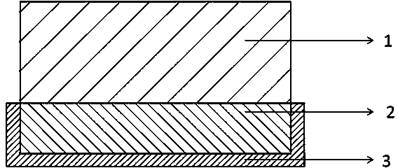
[0053] like figure 1As shown, this product has a three-layer structure: rubber layer 1, metal sheet layer 2, and gold-plated layer 3. The metal base material is a zinc white copper sheet with a thickness of 0.1mm, a HV hardness of 120 to 180, and a copper content of about 55%. . The smooth zinc-nickel-nickel copper sheet is rolled into a fine corrugated sheet by mechanical method, the peak height of the corrugation is 0.1mm, and the peak distance is 0.2mm. Then use an alkaline cleaning solution with a pH value of about 9 to clean and remove oil, wash with water, and then use industrial alcohol to clean and remove oil, then use 12.5% sulfuric acid solution to wash at a temperature of 50 to 80°C for 2 minutes, wash with water, and then , on both sides of the zinc-nickel-nickel copper fine corrugated sheet, use an electroless nickel plating solution containing nickel sulfate and sodium hypophosphite to plate a nickel layer with a thickness of about 2.5 microns. Electroless ni...
Embodiment 2
[0062] The metal foil substrate used was the same as in Example 1. The clean fine corrugated zinc white copper sheet is directly compounded with silicone rubber to form a 1.0mm thick sheet, and then the sheet is punched into small round particles with a diameter of 3.0mm. This small round particle is coated with a layer of 2.5 μm thick nickel, and then the above-mentioned small round particle coated with nickel is plated with gold according to the method of embodiment 1. The prepared gold-plated grains are used as contacts of rubber keys, and have good arc ablation resistance and contact vibration resistance.
Embodiment 3
[0064] The small round grain before gold-plating is the same as embodiment 1. The electroless gold plating solution used is cyanide-free, and its chemical composition is: potassium gold chloride 2.0 g / L, disodium EDTA 20 g / L, potassium citrate 5.0 g / L, sodium lactate 5.0 g / L, thio Sodium sulfate 15g / L, sodium sulfite 15g / L, thiourea 20g / L, sodium tungstate 0.2g / L. Ammonia water is added in an appropriate amount, and the pH value is adjusted to 8.5-9.5 with ammonia water. The bath temperature is 60°C. The electroless plating time is 45 minutes. The contact made in this way also has better performance of arc ablation resistance and contact vibration resistance.
PUM
| Property | Measurement | Unit |
|---|---|---|
| Thickness | aaaaa | aaaaa |
Abstract
Description
Claims
Application Information
 - R&D
- Intellectual Property
- Life Sciences
- Materials
- Tech Scout
- Unparalleled Data Quality
- Higher Quality Content
- 60% Fewer Hallucinations
Browse by: Latest US Patents, China's latest patents, Technical Efficacy Thesaurus, Application Domain, Technology Topic, Popular Technical Reports.
© 2025 PatSnap. All rights reserved.Legal|Privacy policy|Modern Slavery Act Transparency Statement|Sitemap|About US| Contact US: help@patsnap.com

