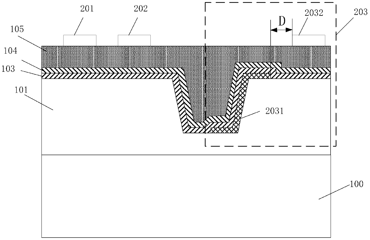
Single-chip three-axis anisotropic magnetoresistive sensor and manufacturing method thereof
An anisotropic magnetic and magnetic sensor technology, applied in the field of magnetic sensors, can solve problems such as difficult process stability, mass production, and low reliability, and achieve good matching, improve reliability, save layout area and process manufacturing costs Effect
- Summary
- Abstract
- Description
- Claims
- Application Information
AI Technical Summary
Problems solved by technology
Method used
Image
Examples
no. 1 example
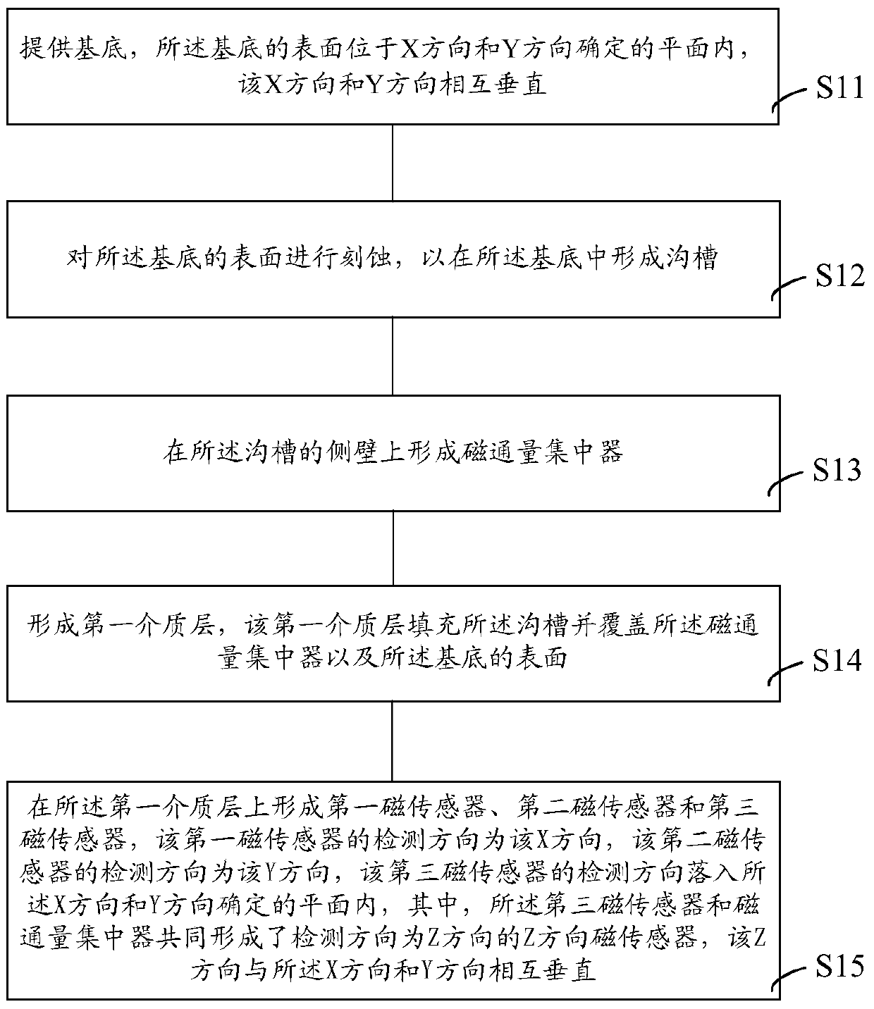
[0075] refer to figure 1 , the manufacturing method of the single-chip three-axis anisotropic magnetoresistive sensor comprises:
[0076] Step S11, providing a substrate, the surface of the substrate is located in a plane determined by the X direction and the Y direction, and the X direction and the Y direction are perpendicular to each other;
[0077] Step S12, etching the surface of the substrate to form grooves in the substrate;
[0078] Step S13, forming a magnetic flux concentrator on the side wall of the groove;
[0079] Step S14, forming a first dielectric layer, the first dielectric layer fills the groove and covers the magnetic flux concentrator and the surface of the substrate;
[0080] Step S15, forming a first magnetic sensor, a second magnetic sensor and a third magnetic sensor on the first medium layer, the detection direction of the first magnetic sensor is the X direction, and the detection direction of the second magnetic sensor is the Y direction, the dete...
no. 2 example
[0094] refer to Figure 9 , providing a base that only includes a semiconductor substrate 300 . The semiconductor substrate 300 can be various conventional semiconductor substrates, for example, it can be a silicon substrate with crystal orientation , and its doping type is not limited, and can be intrinsic, N-type doped or P-type doped. Miscellaneous.
[0095] A silicon oxide layer 301 is formed on the semiconductor substrate 300, the formation method of the silicon oxide layer 301 may be thermal oxidation or chemical vapor deposition (CVD), and its thickness may be between.
[0096] Afterwards, the silicon oxide layer 301 and the semiconductor substrate 300 can be etched in deep grooves by conventional photolithography and etching methods in the microelectronics processing technology. The etching process can be, for example, plasma etching or reactive ion etching, resulting in A groove whose extending direction is perpendicular to the surface of the semiconductor substra...
no. 3 example
[0101] refer to Figure 11 , providing a base that only includes a semiconductor substrate 400 . The semiconductor substrate 400 can be various conventional semiconductor substrates, for example, it can be a silicon substrate with crystal orientation , and its doping type is not limited, and can be intrinsic, N-type doped or P-type doped. Miscellaneous.
[0102] A silicon oxide layer 401 is formed on the semiconductor substrate 340, the formation method of the silicon oxide layer 401 may be thermal oxidation or chemical vapor deposition (CVD), and its thickness may be between.
[0103] After that, the silicon oxide layer 401 can be patterned by conventional photolithography and etching methods in the microelectronic processing technology to form the pattern of the groove; after that, the patterned silicon oxide layer 401 can be used as a mask to The semiconductor substrate 400 is subjected to wet etching. For example, a 5-20% tetramethylammonium hydroxide (TMAH) solution m...
PUM
 Abstract
Description
Claims
Application Information
 - R&D
- Intellectual Property
- Life Sciences
- Materials
- Tech Scout
- Unparalleled Data Quality
- Higher Quality Content
- 60% Fewer Hallucinations
Browse by: Latest US Patents, China's latest patents, Technical Efficacy Thesaurus, Application Domain, Technology Topic, Popular Technical Reports.
© 2025 PatSnap. All rights reserved.Legal|Privacy policy|Modern Slavery Act Transparency Statement|Sitemap|About US| Contact US: help@patsnap.com


