Magnetic tunnel junction
A technology of magnetic tunnel junction and magnetic layer, applied in the field of magnetic tunnel junction, can solve the problems of large lattice mismatch, reduced breakdown voltage, interfacial dislocation and potential barrier defects, etc., and achieves a high tunneling magnetoresistance ratio. Effect
- Summary
- Abstract
- Description
- Claims
- Application Information
AI Technical Summary
Problems solved by technology
Method used
Image

Examples
example 1
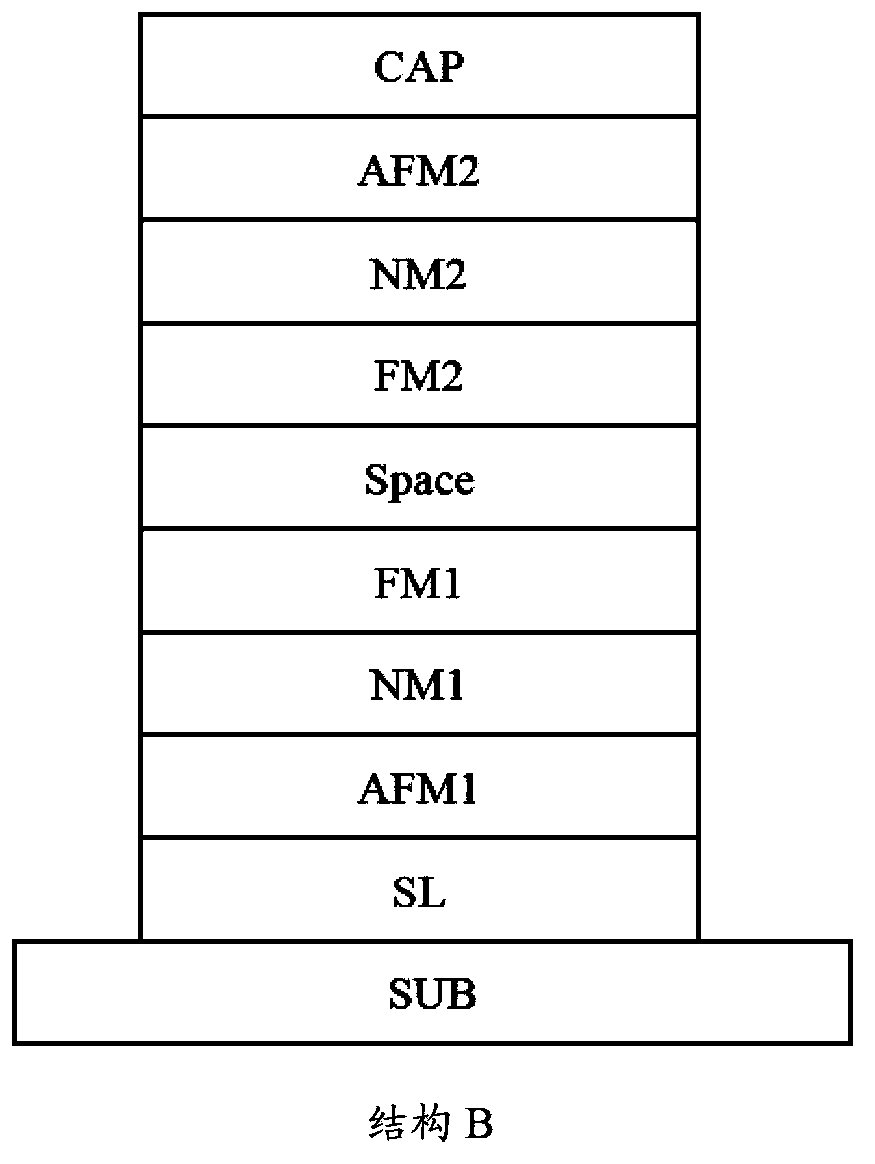
[0079] Magnetic tunnel junction based on spinel oxide single barrier prepared by magnetron sputtering, the structure is Si-SiO 2 / Ta(5nm) / Ru(20nm) / Ta(5nm) / IrMn(15nm) / CoFeB(3nm) / ZnAl 2 o 4 (2nm) / CoFeB(4nm) / Ta(5nm) / Ru(5nm). During deposition, a plane-induced magnetic field of 1000Oe is added, so the magnetization direction of the first magnetic layer is fixed by the antiferromagnetic pinning layer, and the magnetization direction of the second magnetic layer is free.
[0080] (1) Choose a Si-SiO with a thickness of 1mm 2 The substrate is used as the substrate SUB, and the vacuum on the magnetron sputtering equipment is better than 2×10 -6 Pa, the deposition rate is 0.1nm / s, and the argon pressure during deposition is the condition of 0.07Pa, the seed layer SL of Ta(5nm) / Ru(20nm) / Ta(5nm) is deposited on the substrate;
[0081] (2) On the magnetron sputtering equipment, the vacuum is better than 2×10 -6 Pa, the deposition rate is 0.1nm / s, the condition of argon pressure is 0....
example 2
[0092] The structure of the magnetic tunnel junction based on spinel oxide double barrier prepared by magnetron sputtering is:
[0093] Si-SiO 2 / Ta(5nm) / Ru(20nm) / Ta(5nm) / IrMn(15nm) / CoFeB(3nm) / SiZn 2 o 4 (2nm) / CoFeB(4nm) / SiZn 2 o 4 (2nm) / CoFeB(4nm) / IrMn(15nm) / Ta(5nm) / Ru(5nm).
[0094]During deposition, a plane-induced magnetic field of 1000Oe is added, so the magnetization directions of the first magnetic layer and the third magnetic layer are fixed in the same direction by the antiferromagnetic pinning layer, and the magnetization direction of the second magnetic layer is free. The specific preparation method is similar to Example 1.
[0095] Example 3~8:
[0096] The composition and thickness of each layer of the multilayer film of the single-barrier magnetic tunnel junction prepared according to the method of Example 1 are shown in Table 1. Among them, the barrier layer can use spinel oxide barrier, preferably MgAl 2 o 4 , ZnAl 2 o 4 , SiMg 2 o 4 、SiZn 2 o 4 ...
Embodiment 15~19
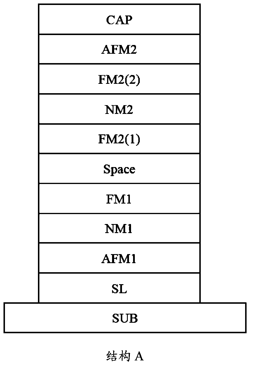
[0106] For the magnetic tunnel junction prepared according to the method of Example 1, the composition and thickness of each layer of the multilayer film are shown in Table 3. Wherein the first and second magnetic layers both adopt antiferromagnetic pinning structure. The structure of the magnetic tunnel junction is SUB / SL / AFM1 / NM1 / FM1 / Space / FM2(1) / NM2 / FM2(2) / AFM2 / CAP, and the composition and thickness of each layer of the multilayer film are shown in Table 3. Among them, the barrier layer can use spinel oxide barrier, preferably MgAl 2 o 4 , ZnAl 2 o 4 , SiMg 2 o 4 、SiZn 2 o 4 , including MgGa 2 o 4 、MgIn 2 o 4 , ZnGa 2 o 4 、ZnIn 2 o 4 、CdAl 2 o 4 , CdGa 2 o 4 、CdIn 2 o 4 、SiCd 2 o 4 , GeMg 2 o 4 、GeZn 2 o 4 、GeCd 2 o 4 , SnMg 2 o 4 , SnZn 2 o 4 , SnCd 2 o 4 etc., the thickness is 0.5~5.0nm; the material and thickness of the two barrier layers can be the same or different; the substrate can be Si substrate, SiC, MgO, GaAs, glass substrate or...
PUM
| Property | Measurement | Unit |
|---|---|---|
| Thickness | aaaaa | aaaaa |
| Thickness | aaaaa | aaaaa |
| Thickness | aaaaa | aaaaa |
Abstract
Description
Claims
Application Information
 - Generate Ideas
- Intellectual Property
- Life Sciences
- Materials
- Tech Scout
- Unparalleled Data Quality
- Higher Quality Content
- 60% Fewer Hallucinations
Browse by: Latest US Patents, China's latest patents, Technical Efficacy Thesaurus, Application Domain, Technology Topic, Popular Technical Reports.
© 2025 PatSnap. All rights reserved.Legal|Privacy policy|Modern Slavery Act Transparency Statement|Sitemap|About US| Contact US: help@patsnap.com