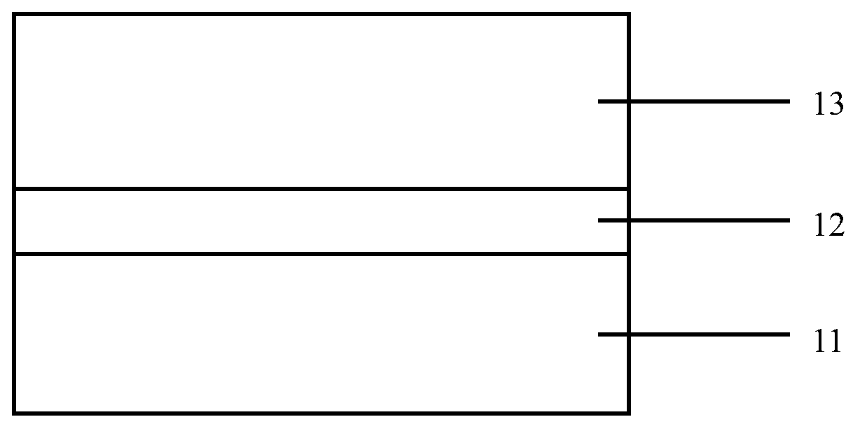
GaN film growing on La0.3Sr1.7AlTaO6 substrate and manufacturing method and application of GaN film
A strontium aluminate tantalum lanthanum and substrate technology, applied in the field of GaN thin film and its preparation, can solve the problems of reducing material carrier mobility, film and substrate cracking, affecting device performance, etc., and achieve carrier radiation High recombination efficiency, repeatability, unique effect of growth process
- Summary
- Abstract
- Description
- Claims
- Application Information
AI Technical Summary
Problems solved by technology
Method used
Image
Examples
Embodiment 1
[0037] A method for preparing a GaN thin film grown on a strontium aluminate tantalum lanthanum substrate, comprising the following steps:
[0038] (1) Selection of the substrate and its crystal orientation: La 0.3 Sr 1.7 AlTaO 6 The substrate, with the (111) plane offset from the (100) direction by 0.5° as the epitaxial plane, the crystal epitaxial orientation relationship is: the (0001) plane of GaN is parallel to the La 0.3 Sr 1.7 AlTaO 6 The (111) surface.
[0039] (2) Surface polishing, cleaning and annealing of the substrate. The specific process of the annealing is: put the substrate into the annealing chamber, and treat La 0.3 Sr 1.7 AlTaO 6 The substrate was annealed for 3 hours and then air-cooled to room temperature;
[0040] The surface polishing of the substrate is specifically:
[0041] La 0.3 Sr 1.7 AlTaO 6 The surface of the substrate is polished with diamond slurry, and the surface of the substrate is observed with an optical microscope until there...
Embodiment 2
[0055] A method for preparing a GaN thin film grown on a strontium aluminate tantalum lanthanum substrate, comprising the following steps:
[0056] (1) Selection of the substrate and its crystal orientation: La 0.3 Sr 1.7 AlTaO 6 The substrate, with the (111) plane offset from the (100) direction by 1° as the epitaxial plane, the crystal epitaxial orientation relationship is: the (0001) plane of GaN is parallel to the La 0.3 Sr 1.7 AlTaO 6 The (111) surface.
[0057] (2) Substrate surface polishing, cleaning and annealing treatment. The specific process of the annealing is: put the substrate into the annealing chamber, and treat La 0.3 Sr 1.7 AlTaO 6 The substrate was annealed for 5 hours and then air-cooled to room temperature;
[0058] The surface polishing of the substrate is specifically:
[0059] La 0.3 Sr 1.7 AlTaO 6 The surface of the substrate is polished with diamond slurry, and the surface of the substrate is observed with an optical microscope until ther...
PUM
| Property | Measurement | Unit |
|---|---|---|
| thickness | aaaaa | aaaaa |
| thickness | aaaaa | aaaaa |
| thickness | aaaaa | aaaaa |
Abstract
Description
Claims
Application Information
 - R&D
- Intellectual Property
- Life Sciences
- Materials
- Tech Scout
- Unparalleled Data Quality
- Higher Quality Content
- 60% Fewer Hallucinations
Browse by: Latest US Patents, China's latest patents, Technical Efficacy Thesaurus, Application Domain, Technology Topic, Popular Technical Reports.
© 2025 PatSnap. All rights reserved.Legal|Privacy policy|Modern Slavery Act Transparency Statement|Sitemap|About US| Contact US: help@patsnap.com


