Process for preparing micro-lens crystal and application of micro-lens crystal
A preparation process and microlens technology, which is applied in lens, printing plate preparation, optics, etc., can solve the problems of difficult to realize public use, narrow application range, slow production speed, etc., and achieve reduced preparation cost, low preparation efficiency and easy operation Effect
- Summary
- Abstract
- Description
- Claims
- Application Information
AI Technical Summary
Problems solved by technology
Method used
Image
Examples
Embodiment 1
[0036] Step 1: Make the grid frame: select 200-mesh mesh yarn and fix it on the screen frame to make a grid frame;
[0037] Step 2: Screen making: First, use a mesh scraper to coat a photosensitive emulsion on the grid to prepare a photosensitive film layer, then dry it with a dryer, repeat the above steps until the photosensitive film layer is 140 μm thick, and the thickness of the photosensitive film layer must be Uniform;
[0038] Step 3: Exposure and washing: Cover the film positive film with the development pattern on the photosensitive film layer, and then expose for 5 minutes. After the exposure is completed, the screen plate is rinsed with water, and the screen will appear on the screen that matches the film positive film. ;
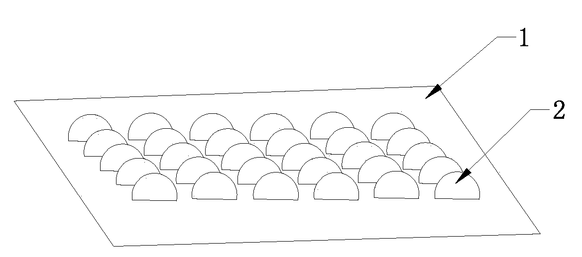
[0039] Step 4: Printing: Select the base material 1, after the screen plate exposed in step 3 is dry, cover the screen plate on the base material 1, and apply transparent UV ink on the screen plate with a scraper, and the UV ink will pass throug...
Embodiment 2
[0043] Step 1: Make the grid frame: select 225-mesh mesh and fix it on the screen frame to make a grid frame;
[0044] Step 2: Screen making: First, use a mesh scraper to coat a photosensitive emulsion on the grid frame to prepare a photosensitive film layer, then dry it with a dryer, repeat the above steps until the photosensitive film layer is 135 μm thick, and the thickness of the photosensitive film layer must be Uniform;
[0045] Step 3: Exposure and washing: Cover the film positive film with the development pattern on the photosensitive film layer, and then expose for 5 minutes. After the exposure is completed, the screen plate is rinsed with water, and the screen will appear on the screen that matches the film positive film. ;
[0046] Step 4: Printing: Select the base material 1, after the screen plate exposed in step 3 is dry, cover the screen plate on the base material 1, and apply transparent UV ink on the screen plate with a scraper, and the UV ink will pass throu...
Embodiment 3
[0050] Step 1: Make the grid frame: select 250-mesh mesh and fix it on the screen frame to make a grid frame;
[0051] Step 2: Screen making: First, use a mesh scraper to coat a photosensitive emulsion on the grid frame to prepare a photosensitive film layer, then dry it with a dryer, repeat the above steps until the photosensitive film layer is 115 μm thick, and the thickness of the photosensitive film layer must be Uniform;
[0052] Step 3: Exposure and washing: Cover the film with a developing pattern on the photosensitive film layer, and then expose for 7 minutes. After the exposure is completed, the screen is rinsed with water, and the screen will appear on the screen that matches the film. ;
[0053] Step 4: Printing: Select the base material 1, after the screen plate exposed in step 3 is dry, cover the screen plate on the base material 1, and apply transparent UV ink on the screen plate with a scraper, and the UV ink will pass through The mesh adheres to the substrate...
PUM
 Abstract
Description
Claims
Application Information
 - R&D
- Intellectual Property
- Life Sciences
- Materials
- Tech Scout
- Unparalleled Data Quality
- Higher Quality Content
- 60% Fewer Hallucinations
Browse by: Latest US Patents, China's latest patents, Technical Efficacy Thesaurus, Application Domain, Technology Topic, Popular Technical Reports.
© 2025 PatSnap. All rights reserved.Legal|Privacy policy|Modern Slavery Act Transparency Statement|Sitemap|About US| Contact US: help@patsnap.com

