
Air gap forming method between integrated circuit (IC) interconnector and interlevel dielectric layer

A technology of interlayer dielectric layer and air space, applied in electrical components, semiconductor/solid-state device manufacturing, circuits, etc., can solve problems such as limiting operating speed, and achieve the effect of reducing RC delay, speeding up signal transmission, and reducing the effect of capacitance

Active Publication Date: 2015-04-01
SEMICON MFG INT (SHANGHAI) CORP
View PDF7 Cites 0 Cited by
  • Summary
  • Abstract
  • Description
  • Claims
  • Application Information

AI Technical Summary

Problems solved by technology

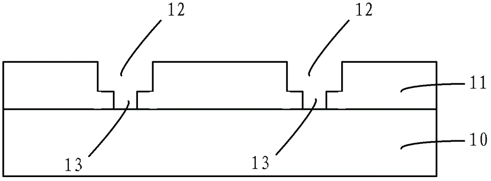
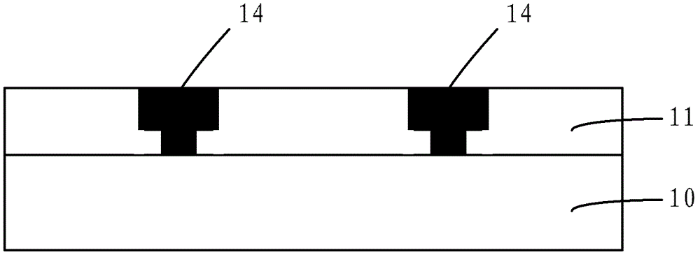
Due to the existence of this structure, the interconnection 14 will be affected by the RC delay during signal transmission, thus limiting the operating speed of the IC

Method used


Image

  • Air gap forming method between integrated circuit (IC) interconnector and interlevel dielectric layer
  • Air gap forming method between integrated circuit (IC) interconnector and interlevel dielectric layer
  • Air gap forming method between integrated circuit (IC) interconnector and interlevel dielectric layer

Examples


Embodiment Construction

[0034] In order to make the object, technical solution and advantages of the present invention clearer, the present invention will be further described in detail below with reference to the accompanying drawings and examples.

[0035] The steps of the content of the present invention are as Figure 4 shown, refer to Figure 4 and Figure 5 to Figure 13 As shown, the implementation process of the specific embodiment includes the following contents.

[0036] Step 1: If Figure 5 As shown, a semiconductor device 10 such as CMOS is provided, and a first dielectric barrier layer (dielectric barrier) 15 and an interlayer dielectric layer 11 are sequentially formed on the semiconductor device 10 .

[0037] Wherein, the first dielectric barrier layer 15 is made of silicon nitride carbide material, and the thickness can be It is formed by plasma enhanced chemical vapor deposition (PECVD, Plasma Enhanced Chemical Vapor Deposition). The functions of the first dielectric barrier lay...


PUM


Abstract

The invention discloses an air gap forming method between an integrated circuit (IC) interconnector and an interlevel dielectric layer. The air gap forming method comprises the steps of providing a semiconductor component, sequentially forming a first dielectric barrier layer and the interlevel dielectric layer on the semiconductor component, etching a sacrificial area on the interlevel dielectric layer, wherein the sacrificial area is exposed out of the first dielectric barrier layer, depositing oxide in the sacrificial area, etching a part of the oxide, forming a groove, continuously etching the oxide and the first dielectric barrier layer in the groove until source and drain regions or a grid electrode of the semiconductor component are exposed, forming a through hole, plating the interconnector inside the groove and the through hole in an electrochemical mode, eliminating the remaining oxide, and forming an air gap. According to the air gap forming method, the air gap is formed between the interconnector and the interlevel dielectric layer, and therefore a capacitance effect of the interconnector is reduced. Furthermore, resistance-capacitance (RC) delay of the interconnector is reduced, and signal transmission speed of the interconnector is accelerated.

Description

technical field [0001] The invention relates to semiconductor manufacturing technology, in particular to a method for forming an air gap (air gap) between an IC interconnection (interconnection) and an interlayer dielectric layer (ILD, interlayerdielectric). Background technique [0002] As the size of IC (Integrated Circuit, integrated circuit) becomes smaller and smaller, the RC delay generated between metal lines such as interconnection (interconnection) gradually replaces the delay of the transistor itself and becomes the main factor limiting the operating speed of the IC. . The speed of signal transmission in the circuit is affected by the product of resistance R and capacitance C. The larger the RC product, the slower the speed and the higher the delay. Conversely, the smaller the RC product, the faster the signal transmission speed and the delay lower. For an interconnection (such as a copper interconnection), its resistance R is determined by its own material prope...

Claims


Application Information

Patent Timeline
Patent Type & Authority Patents(China)
IPC IPC(8): H01L21/768
Inventor 鲍宇
Owner SEMICON MFG INT (SHANGHAI) CORP
Learn More