
Method and application of growing ultra-thin high-quality oxide films on two-dimensional layered materials

An oxide film, two-dimensional layered technology, applied in metal material coating process, coating, gaseous chemical plating, etc. Effects of alleviation of short channel effects, reduced capacitance effects, excellent uniformity and withstand voltage

Active Publication Date: 2020-07-31
NANJING UNIV
View PDF5 Cites 0 Cited by
  • Summary
  • Abstract
  • Description
  • Claims
  • Application Information

AI Technical Summary

Problems solved by technology

[0005] Purpose of the invention: Aiming at the problems of damage to the two-dimensional material, inhomogeneous, discontinuous, and non-dense oxide films existing in the methods for growing oxide films on two-dimensional materials in the prior art, the present invention provides a two-dimensional layered A method for growing an ultra-thin high-quality oxide film on a material, and providing an application of the method for preparing an electronic device

Method used


Image

  • Method and application of growing ultra-thin high-quality oxide films on two-dimensional layered materials
  • Method and application of growing ultra-thin high-quality oxide films on two-dimensional layered materials
  • Method and application of growing ultra-thin high-quality oxide films on two-dimensional layered materials

Examples


Embodiment 1

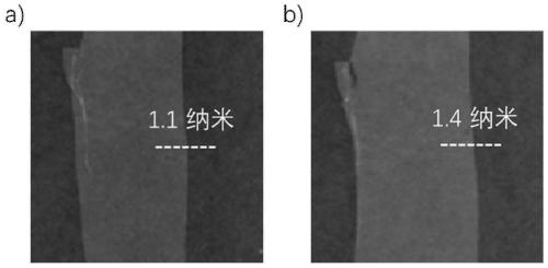
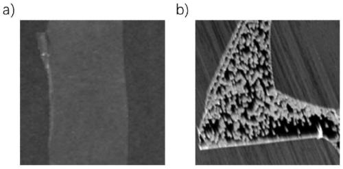
[0032]1) The graphene two-dimensional layered material is prepared by mechanical exfoliation, and the graphene two-dimensional layered material is transferred to a silicon wafer, and upper source and drain electrodes are prepared on both sides of the graphene; as figure 1 (a), Thin graphene transferred onto a silicon wafer as a substrate with a thickness of 1.1 nm.

[0033] 2) Put 3,4,9,10-perylenetetraic acid dianhydride powder into a quartz boat as a growth source, and put the quartz boat into the center of the tube furnace; place the silicon wafer transferred with graphene on another on the quartz boat, and put the quartz boat into the quartz tube, 2 cm away from the quartz boat containing the 3,4,9,10-perylenetetraic acid dianhydride powder; after placing, install the quartz tube into the tube type corresponding position of the furnace, and vacuumize;

[0034] 3) Start the tube furnace, raise the temperature of the furnace body to 240°C in 10 minutes, then raise the tempe...

Embodiment 2

[0046] 1) The graphene two-dimensional layered material is prepared by mechanical exfoliation, and the graphene two-dimensional layered material is transferred to a silicon wafer;

[0047] 2) Put 3,4,9,10-perylenetetraic acid dianhydride powder into a quartz boat as a growth source, and put the quartz boat into the center of the tube furnace; place the silicon wafer transferred with graphene on another on the quartz boat, and put the quartz boat into the quartz tube, 2 cm away from the quartz boat containing the 3,4,9,10-perylenetetraic acid dianhydride powder; after placing, install the quartz tube into the tube type corresponding position of the furnace, and vacuumize;

[0048] 3) Start the tube furnace, raise the temperature of the furnace body to 240°C in 10 minutes, then raise the temperature to 260°C in 5 minutes, and maintain it at 260°C for 0.8 hours, the growth source of 3,4,9,10-perylenetetraacid dianhydride powder evaporates , and deposited on the graphene; after t...

Embodiment 3

[0053] 1) The graphene two-dimensional layered material is prepared by mechanical exfoliation, and the graphene two-dimensional layered material is transferred to a silicon wafer;

[0054] 2) Put 3,4,9,10-perylenetetraic acid dianhydride powder into a quartz boat as a growth source, and put the quartz boat into the center of the tube furnace; place the silicon wafer transferred with graphene on another on the quartz boat, and put the quartz boat into the quartz tube, 2 cm away from the quartz boat containing the 3,4,9,10-perylenetetraic acid dianhydride powder; after placing, install the quartz tube into the tube type corresponding position of the furnace, and vacuumize;

[0055] 3) Start the tube furnace, raise the temperature of the furnace body to 240°C in 10 minutes, then raise the temperature to 260°C in 5 minutes, and maintain it at 260°C for 0.2 hours, the growth source of 3,4,9,10-perylenetetraacid dianhydride powder evaporates , and deposited on the graphene; after t...


PUM

PropertyMeasurementUnit
thicknessaaaaaaaaaa
thicknessaaaaaaaaaa
thicknessaaaaaaaaaa

Abstract

The invention discloses a method for growing an ultra-thin high-quality oxide thin film on a two-dimensional layered material and an application thereof. The method comprises the following steps of (1) growing a single-layer organic dye molecular thin film on the two-dimensional layered material by adopting a van der waals epitaxial growth technology; (2) using an atomic layer deposition technology, taking the single-layer organic dye molecular thin film as a seed layer, and growing an ultra-thin uniform oxide thin film on the two-dimensional layered material. According to the method for growing the ultra-thin high-quality oxide thin film on the two-dimensional layered material and the application thereof, the single-layer organic dye molecular thin film grows on the surface of the two-dimensional layered material through the van der waals epitaxy to serve as the seed layer, the two-dimensional layered material can be almost not damaged, and the ultra-thin and uniform dense high-quality oxide thin film can be deposited on the seed layer; and meanwhile, the growth method is low in cost and easy to process and implement; the oxide thin film prepared by the method disclosed by the invention can be very thin, still maintain excellent uniformity and pressure resistance, and can be applied to electronic devices in various forms.

Description

technical field [0001] The invention relates to a method for growing an ultra-thin high-quality oxide film on a two-dimensional layered material and its application for preparing electronic devices, belonging to the field of two-dimensional material electronic devices. Background technique [0002] In recent decades, silicon-based electronic devices have been shrinking in feature size under the guidance of Moore's Law. However, as the scale gradually approaches the quantum limit, problems including short-channel effects limit the further reduction in the size of silicon-based electronic devices. Research and development of new materials is one of the main ways to continue Moore's Law. Since the discovery of graphene, more and more two-dimensional layered materials have attracted people's attention due to their excellent properties in terms of force, heat, light, and electricity. Two-dimensional materials are generally bonded by covalent bonds in the plane, while the interl...

Claims


Application Information

Patent Timeline
Patent Type & Authority Patents(China)
IPC IPC(8): C23C16/02C23C14/12C23C14/24C23C16/40C23C16/455H01L21/28
CPCC23C14/12C23C14/24C23C16/0272C23C16/40C23C16/45525H01L21/28194
Inventor 王欣然李卫胜周健于志浩施毅
Owner NANJING UNIV
Learn More