
Electrostatic discharge protection device

An electrostatic discharge, ESD protection technology, applied in circuit devices, emergency protection circuit devices, emergency protection circuit devices for limiting overcurrent/overvoltage, etc., can solve problems such as affecting RF input matching and reducing performance

Active Publication Date: 2014-09-10
TAIWAN SEMICON MFG CO LTD
View PDF3 Cites 0 Cited by
  • Summary
  • Abstract
  • Description
  • Claims
  • Application Information

AI Technical Summary

Problems solved by technology

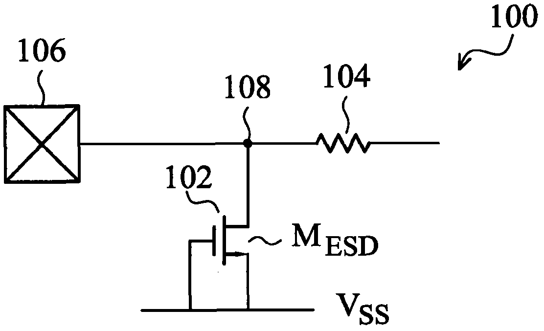
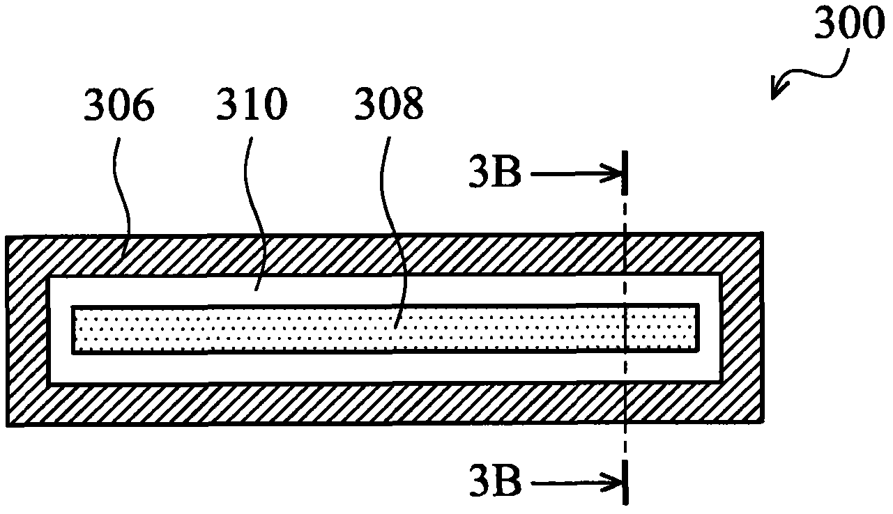
Although the STI diode 300 provides low capacitance and small area, its parasitic capacitance and resistance affect the RF input match and degrade performance in high frequency RF applications

Method used


Image

  • Electrostatic discharge protection device
  • Electrostatic discharge protection device
  • Electrostatic discharge protection device

Examples


Embodiment Construction

[0048] The invention discloses an improved electrostatic discharge (ESD) protection device for radio frequency applications. ESD protection devices include junction varactors that act as voltage-dependent capacitors when reverse biased. The bias voltage of the junction varactor may be optimized to minimize capacitance to reduce the capacitive effects of network matching during normal RF operation. During an ESD event, the junction varactor is forward biased and acts as an ESD protection diode to shunt the ESD current. In addition, the junction varactor provides sufficient metal width and a sufficient amount of vias and contacts to avoid electromigration, and has a length-to-width (L / W) ratio that allows alignment with the bond pad edge, Compared with traditional ESD protection devices, it has improved circuit layout.

[0049] Figure 4A is a cross-sectional view of a junction varactor 400A for ESD protection for RF applications. like Figure 4A As shown, junction varactor...


PUM


Abstract

The invention provides an electrostatic discharge protection device, which includes: a first well of a first semiconductor type formed in a substrate of a second semiconductor type to form a first diode. A second well of a second semiconductor type is formed in the substrate to form a second diode with the first well. A first plurality of doped regions of the first semiconductor type are formed on the upper surface of the first well. A second plurality of doped regions of the second semiconductor type are formed on the upper surface of the first well to form a third diode having the first well. A plurality of shallow trench isolation STI regions are disposed on the upper surface of the first well, and each STI region is disposed between the doped regions of the first semiconductor type and the second semiconductor type. The third diode provides a current bypass when an ESD voltage spike is received at one of the first or second multi-doped regions. The present invention can be optimized to reduce the capacitive effects of network matching during normal radio frequency operation, and has improved circuit layout.

Description

technical field [0001] The present invention relates to an integrated circuit, and in particular to electrostatic discharge (ESD) protection of a radio frequency (radio frequency, RF) integrated circuit. Background technique [0002] With the miniaturization of integrated circuit devices, the current trend is to produce structures with shallower junction depths, thinner gate oxide layers, lightly-doped drain (LDD) structures, shallow trench isolation structures (shallow trench isolation (STI), and self-aligned metal-silicon compound (salicide) processed integrated circuits, which are used in advanced quarter-sub-micron (sub-quarter-micron) complementary metal oxide semiconductor (CMOS) technology. These processes cause related CMOS IC products to become more susceptible to ESD damage. Therefore, an ESD protection circuit is built in the chip to protect the device and the circuit from ESD damage. For RF ICs, EDS protection is particularly challenging in terms of reducing g...

Claims


Application Information

Patent Timeline
Patent Type & Authority Patents(China)
IPC IPC(8): H02H9/04H01L23/60H01L27/04
CPCH01L27/0255H01L2924/0002H01L2924/00
Inventor 蔡铭宪叶子祯周淳朴薛福隆
Owner TAIWAN SEMICON MFG CO LTD
Learn More