Batch Productivity Improvement Method for Homogeneous Bonding System of Multi-chip Module

A multi-chip component and homogeneous bonding technology, which is applied in the direction of electrical components, electric solid devices, semiconductor devices, etc., can solve the problems of no homogeneous bonding system, easy electromigration, and no application for multi-chip components. To achieve the effect of improving the ability to work fully and reliably for a long time, broad market prospects and application space, and improving the manufacturability of large quantities

Active Publication Date: 2016-01-13
GUIZHOU ZHENHUA FENGGUANG SEMICON
View PDF3 Cites 0 Cited by
  • Summary
  • Abstract
  • Description
  • Claims
  • Application Information

AI Technical Summary

Problems solved by technology

[0003] The defects or main problems of the original technology are as follows: ①In the silver conduction band and palladium-silver conduction band, silver is easy to oxidize, and in the case of long-term power-on, it is easy to produce electromigration phenomenon, which seriously affects the reliability of the device, usually manifested as Bonding strength declines; ②Gold conduction band is in the case of high current, in the Au-Al bonding system, the electromigration phenomenon of the gold layer in the bonding contact area is obvious, and "purple spots" are easily formed between Au-Al, and the product composition is AuAl 2 , resulting in the loosening and voiding of the alloy points formed during Au-Al bonding, and the final bonding force is greatly reduced; ③ In the gold-aluminum bonding system at high temperature, due to the diffusion of gold into aluminum, "white spots" are formed between Au-Al, The product is Au 2 Al, Au 5 al 2 、Au 5 Al, forming a layer of brittle and insulating intermetallic compound (that is, gold-aluminum compound), this product can greatly reduce the conductivity of the alloy point, and can form an open circuit in severe cases; ④ chip (the surface metal layer is an aluminum layer), conduction band ( It is difficult to be compatible with the respective requirements in the bonding process between the lead post (gold-plated or nickel-plated), the lead wire (gold wire or silicon-aluminum wire); ⑤ thick film conduction tape, thick film The surface roughness of the bonding area is relatively large, and the bonding tension and long-term reliability of the bonding system are poor in quality consistency.
Therefore, multi-chip components produced by gold-aluminum (Au-Al) and silver-aluminum (Ag-Al) heterogeneous bonding systems cannot be used in high-reliability occasions, and nickel-aluminum (Ni-Al) heterogeneous bonding The bonding quality of the system is relatively reliable, but compared with the homogeneous bonding system, there is still a certain gap. The multi-chip components produced by the nickel-aluminum (Ni-Al) heterogeneous bonding system cannot be used in aerospace-grade high-end reliable field
[0004] After searching, there are 20 patent applications involving multi-chip components, but there are no applications for multi-chip components involving homogeneous bonding systems, let alone homogeneous bonds Application documents for integrated system ceramic thick film multi-chip modules

Method used


Image

  • Batch Productivity Improvement Method for Homogeneous Bonding System of Multi-chip Module
  • Batch Productivity Improvement Method for Homogeneous Bonding System of Multi-chip Module
  • Batch Productivity Improvement Method for Homogeneous Bonding System of Multi-chip Module

Examples


Embodiment 1

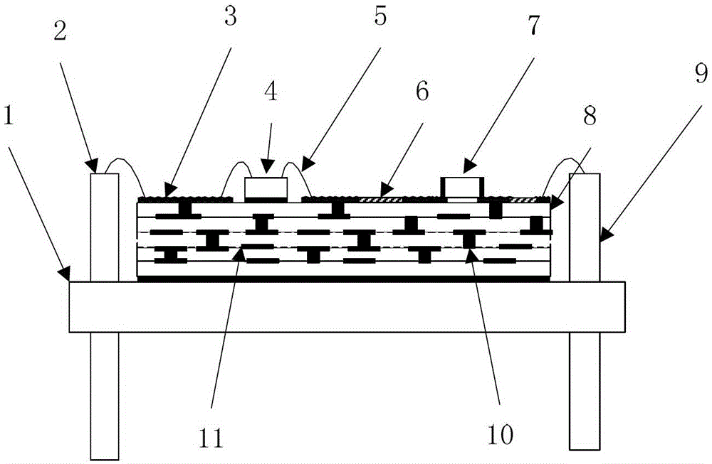
[0018] Example 1 : The original process such as Figure 6 , the process is as follows:

[0019] (1) Material preparation: prepare green ceramic sheets, gold conductor paste, ruthenium resistance paste, semiconductor chips, etc.;

[0020] (2) Cutting: According to the size of the specific product LTCC substrate, cut the pieces according to the requirements;

[0021] (3) Punching: Each layer is interconnected through through holes and conduction bands. Using mechanical punching method, the interconnection path between the ceramic sheets of the LTCC substrate is made according to the graphic and aperture of the product design;

[0022] (4) Hole filling and guide band printing: fill the metal paste into the via holes by screen printing on the ceramic sheet, print out the guide band pattern according to the specified pattern, and dry (150°C, 10min);

[0023] (5) Stopband printing: Print the resistive paste into the stopband pattern according to the specified pattern by screen ...

Embodiment 2

[0037] Example 2: the present invention process such as Figure 7 , add thick film conduction band sintering, mechanical leveling, cleaning and drying processes between thick film conduction band printing and drying and curing, and thick film stop band printing. The added process is as follows:

[0038] (1) Prepare a gold polishing solution with an abrasive grain hardness of 25GPa±5GPa and a particle diameter of 50nm±10nm;

[0039] (2) Conduction band sintering (875°C, 12min, total time 45min);

[0040] (3) Perform one-time chemical mechanical polishing on all gold conduction bands and gold bonding areas with a rotary polishing machine, and the surface flatness is controlled within 0.1 microns;

[0041] (4) Cleaning and drying with deionized water;

[0042] (5) Printing, sintering and resistance adjustment process of resistance paste.

[0043] After the trimming and testing of the thick film resistors, the aluminum metal film deposition process in the gold thick film bondin...


PUM

PropertyMeasurementUnit
particle diameteraaaaaaaaaa
thicknessaaaaaaaaaa

Abstract

The present invention has disclosed the method of batching the production of the altitude key system of the ceramic thick film multi -chip component. It is achieved by using the overall chemical mechanical polishing method.Overall polishing, and then use mechanical mold covering methods to form a layer of aluminum film on the surface of the keyheed area. According to the conventional integrated process, the chip and chip component are integrated on the processing substrate that is processed.The synthesis is combined with silicon-aluminum filament, and the tube foot and the substrate use the golden keys; the surface flatness of all the keys on the top layer of the ceramic substrate is controlled at ≤0.1 μm at the same time.The surface of the Golden Bate area of the present invention is one-time polished and flattened, which simultaneously improves the reliability of the substrate and the golden bonding of the substrate and the tube.The key system, improve the ability of multi -chip components to fully reliable for a long time; improve the mass production of multi -chip components.

Description

technical field [0001] The invention relates to a multi-chip module (abbreviated as MCM), specifically, to a ceramic thick-film multi-chip module (abbreviated as MCM-C), and further to a homogenous bonding system ceramic thick-film multi-chip module. Background technique [0002] In the original multi-chip module integration technology, gold paste, silver paste or palladium-silver paste, etc. The conductive paste and the ruthenium-based resistor paste are formed on the LTCC substrate to form conduction band and stop band patterns according to the requirements of the top layer layout design, and then formed after high-temperature sintering. At the end of the conduction band, or at a designated place, form a bonding area, a semiconductor chip assembly area, or other chip component assembly areas, and the rest of the area (including the thick film stop band) is protected by a glass uranium insulating layer. Assembly of semiconductor chips and other chip components on the subst...

Claims


Application Information

Patent Timeline
Patent Type & Authority Patents(China)
IPC IPC(8): H01L21/60
CPCH01L2224/45124H01L2224/45144H01L2224/48091H01L2224/48227H01L2224/73265H01L2924/19105H01L2924/19107
Inventor 杨成刚苏贵东
Owner GUIZHOU ZHENHUA FENGGUANG SEMICON
Why Eureka
Try Eureka