Eureka AIR delivers breakthrough ideas for toughest innovation challenges, trusted by R&D personnel around the world.

Linear doped spin field-effect tube (Spin-FET)

A field effect tube and linear doping technology, which is applied in the direction of electrical components, circuits, semiconductor devices, etc., can solve the problems of enhancement and device performance degradation, and achieve the effects of enhanced capacity, high magnetic current rate, and low off-state current

Inactive Publication Date: 2013-05-08
NANJING UNIV OF POSTS & TELECOMM
View PDF0 Cites 4 Cited by
  • Summary
  • Abstract
  • Description
  • Claims
  • Application Information

AI Technical Summary

Problems solved by technology

[0005]Technical problem: The purpose of this invention is to provide a linear Doped spin field effect transistors enhance the device's ability to suppress hot carrier effects

Method used


Image

  • Linear doped spin field-effect tube (Spin-FET)

Examples


Embodiment Construction

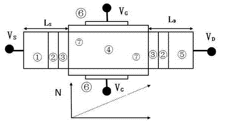
[0014] The spin field effect transistor of the MOSFET-like structure researched by the present invention is shown in the summary figure, the spin field effect transistor of linear doping of the present invention is a kind of double gate 6 structure, wherein uses semiconductor material silicon 4 as conductive channel, The channel and the two gate electrodes are filled with the same dielectric material, and the two gate electrodes form a symmetrical structure centered on the channel; the source and drain regions of the field effect transistor are half-metal ferromagnetic, and the silicon 4 channel There is a layer of spin random layer 2 and tunnel oxide layer 3 between the source region and the drain region, and there is a linear doping structure in the silicon 4 channel, that is, linear doping is performed in the channel. The double gate 6 is a top gate and a bottom gate symmetrical about the device channel, which adopts a metal with a work function of 3.95 as the gate material,...


PUM


Abstract

The invention discloses a spin field-effect tube (Spin-FET) with a linear light dope structure. A transport model which is suitable for the linear doped Spin-FET is constructed based on the quantum mechanics nonequilibrium green function theoretical framework and through the self-consistent solving Poisson and the Schrodinger equation, and the influence of a linear doping strategy and a common doping strategy on the electrical properties of the Spin-FET is calculated by using the model. Compared with the electrical properties of other doping strategies such as output characteristics, transfer characteristics, switch current ratio and magnetism current rate, the linear doped Spin-FET has larger switch current ratio, higher magnetism current rate, and smaller sub-threshold swing and threshold voltage drift. Not only can show that linear doping has better grid control capability, but also short-channel effect and hot carrier effect can be effectively restrained.

Description

technical field [0001] The invention relates to the field of spin field effect transistors, in particular to spin field effect transistors with a linear doping structure. Background technique [0002] In addition to charge, another property of electrons is spin. Conventional semiconductor devices only exploit the charge properties of electrons while neglecting the spin properties. At present, as the size of semiconductor devices is approaching the limit, spintronics (Spintronics) further considers the new characteristic of spin on the basis of traditional semiconductor devices, and uses electron spin to control electrons. The use of spintronics to develop new electronic devices has become a new discipline. [0003] In 1990, Datta and Das first proposed the spin field effect transistor, which is a sandwich-like structure composed of ferromagnetic / semiconductor / ferromagnetic. G.Schmidt researched that the spin injection rate is not high due to the mismatch between the condu...

Claims


Application Information

Patent Timeline
Patent Type & Authority Applications(China)
IPC IPC(8): H01L29/66H01L29/10
Inventor 王伟王燕张华鑫
Owner NANJING UNIV OF POSTS & TELECOMM
Why Eureka
Eureka Blog
Learn More