Polycrystalline SiTFT of multi-grid double-channel structure

A polysilicon thin film, dual-channel technology, applied in transistors and other directions, can solve problems such as increasing the aspect ratio

Inactive Publication Date: 2005-03-16
JILIN UNIV
View PDF0 Cites 10 Cited by
  • Summary
  • Abstract
  • Description
  • Claims
  • Application Information

AI Technical Summary

Problems solved by technology

The off-state leakage current of the TFT with the LDD structure and the double gate structure is small, but to achieve the current required to drive the OLED, the aspect ratio must be increased, which is in contradiction with the high resolution requirement of the OLED

Method used


Image

  • Polycrystalline SiTFT of multi-grid double-channel structure
  • Polycrystalline SiTFT of multi-grid double-channel structure
  • Polycrystalline SiTFT of multi-grid double-channel structure

Examples


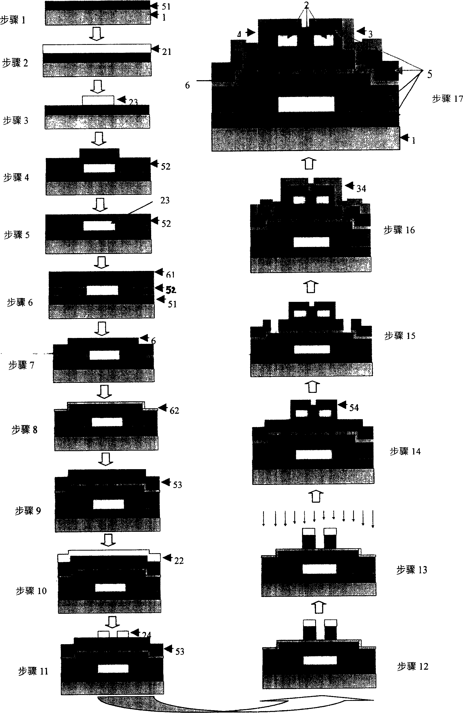
preparation Embodiment 1

[0048] 1) First, use PECVD method on the silicon substrate at 300°C to obtain 5000 Å of SiO 2 .

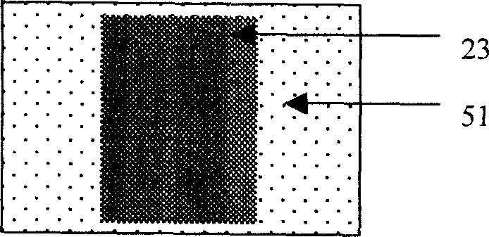
[0049] 2) Use LPCVD method on the substrate (atmospheric pressure 0.3Torr, SiH 4 60 sccm, the speed is 25 Å per second) to deposit 2000 Å of a-Si (amorphous silicon, SiH 4 Decomposed as a gas source to obtain a-Si, the substrate temperature during deposition is 200°C, and the background vacuum is 2×10 -4 Pa, reaction chamber pressure 80Pa) and ion implantation doping (energy 45KeV, concentration 5×10 15 cm -2 ), then use plasma etching process (dry etching) photolithography such as figure 2 The pattern shown forms the bottom gate 23;

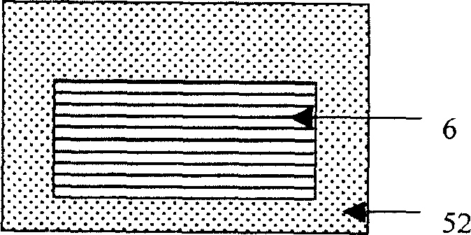
[0050] 3) Precipitate 2500 Å of SiNx as the insulating layer of the bottom gate. The growth of this layer of film is also performed on SiH by PECVD 4 and NH 3 grow under a mixed atmosphere, the substrate temperature is kept at 270°C, and the reaction chamber pressure is 30Pa;

[0051] 4) Precipitating a 500 Å a-Si thin film by LPCVD technol...


PUM


Abstract

The invention relates to silicon polycrystal film transistor with multi-gate tow-channel structure, comprising insulating substrate (1) , SiO2 cushion layer (51), gate electrode insulating layer (53), two top gate electrodes (24) in gate electrode insulating layer (53) , drain region (3) and source region (4), gate electrode insulating layer (52) on SiO2 cushion layer (51), bottom gate electrode (23) on gate electrode insulating layer (52), bottom gate electrode (23) and top gate electrode (24) are connected by linking hole of gate electrode (25), and channel (6) formed by silicon polycrystal film on gate electrode insulating layer (52). The invention of TFT component has the same extent of close drain current of TFT made in the same condition, besides, it has more advantages such as open current increased by one time, better drive capability for load than TFT which has the same ratio of width and length, smaller area in integration matrix when supplies the same current, and increasing opening rate.

Description

technical field [0001] The invention belongs to the technical field of semiconductors, and in particular relates to a polysilicon thin-film transistor (TFT) which can be used for a drive array of a polysilicon (Poly-Si) active organic electroluminescence display (Active Matrix Organic Light Emitting Diode, referred to as AMOLED) and a peripheral drive array. , Thin FilmTransistor), can also be used for polysilicon active liquid crystal display (AM LCD) drive array and peripheral drive array polysilicon thin film transistor (P-Si TFT). Background technique [0002] There are many kinds of TFT structures used in Poly-Si AM OLED, the most common ones are: self-aligned (Self-align) structure, gate offset (Off-set) structure, drain lightly doped (LDD) structure and Dual gate (dual-gate) structures have their own advantages and scope of application. Although the self-aligned structure is simple and easy to implement, the off-state leakage current is large; although the gate offse...

Claims


Application Information

Patent Timeline
IPC IPC(8): H01L29/786
Inventor 王丽杰张彤李传南赵毅侯晶莹刘式墉
Owner JILIN UNIV
Why Eureka
Try Eureka