Method for implementing light emitting diode surface pattern preparation by using two-beam interference for assisting wet etching

A technology of light-emitting diodes and double-beam interference, used in semiconductor devices, electrical components, circuits, etc., can solve the problems of window layer structure damage, complex process, p-GaP surface damage, etc., to improve speed, simple operation, and applicability strong effect

Inactive Publication Date: 2013-04-03
SHANDONG UNIV
View PDF6 Cites 4 Cited by
  • Summary
  • Abstract
  • Description
  • Claims
  • Application Information

AI Technical Summary

Problems solved by technology

The disadvantage of this method is that (1) this method needs to pass SiO 2 The steps of deposition of protective layer, noble metal sputtering and heat treatment, plasma etching, and cleaning of protective layer and noble metal layer are very complicated and expensive, and large-scale application cannot be realized; (2) plasma etching Corrosion will cause certain damage to the structure of the window layer and affect the electrical performance of the LED
The disadvantage of this method is that (1) it is necessary to prepare an ITO mask and corrode the prepared ITO mask into ITO particles. This process is relatively complicated and the cost of red LEDs is much higher than that of the normal process; (2 ) The ITO particles formed in this method are random, so the corrosion structure formed is also random, and a periodic structure cannot be formed; (3) The ICP etching technology used in this method will cause damage to the p-GaP surface and destroy the p- Electrical properties of GaP
However, in this technology, only the random etching of the p-GaP window layer is realized, and a random etching structure is prepared on the surface of p-GaP, and a periodic surface pattern structure cannot be prepared.
[0008] None of the above technologies and patents can produce a surface with a periodic structure, and the mask and photolithography technology will greatly increase the cost of light-emitting diodes

Method used


Image

  • Method for implementing light emitting diode surface pattern preparation by using two-beam interference for assisting wet etching
  • Method for implementing light emitting diode surface pattern preparation by using two-beam interference for assisting wet etching
  • Method for implementing light emitting diode surface pattern preparation by using two-beam interference for assisting wet etching

Examples


Embodiment

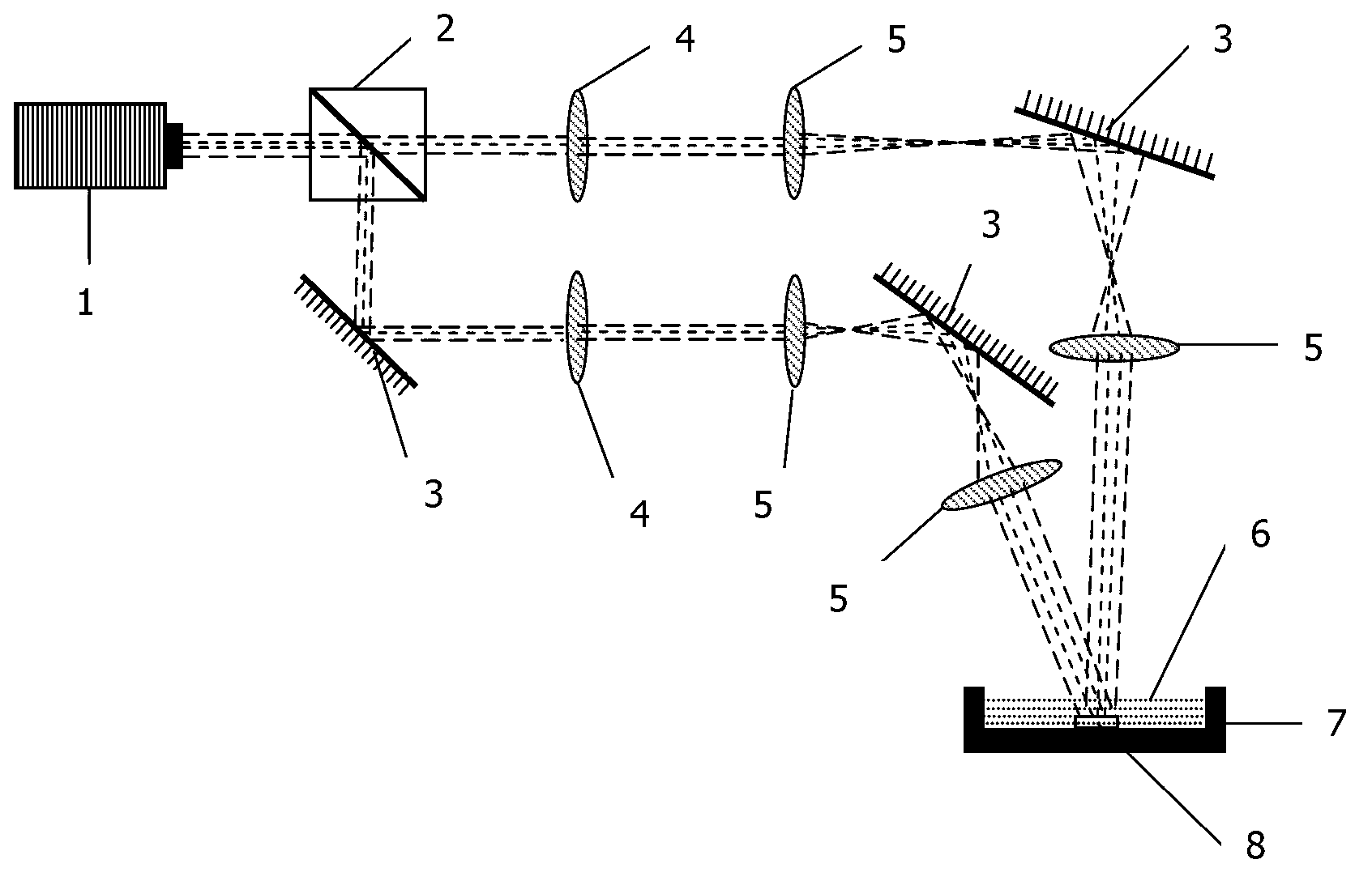
[0048] like Figure 1-Figure 5 shown.

[0049] A method for preparing surface patterns of light-emitting diodes by using double-beam interference-assisted wet etching. Taking the surface pattern preparation of AlGaInP red light-emitting diode epitaxial wafers as an example, the steps are as follows:

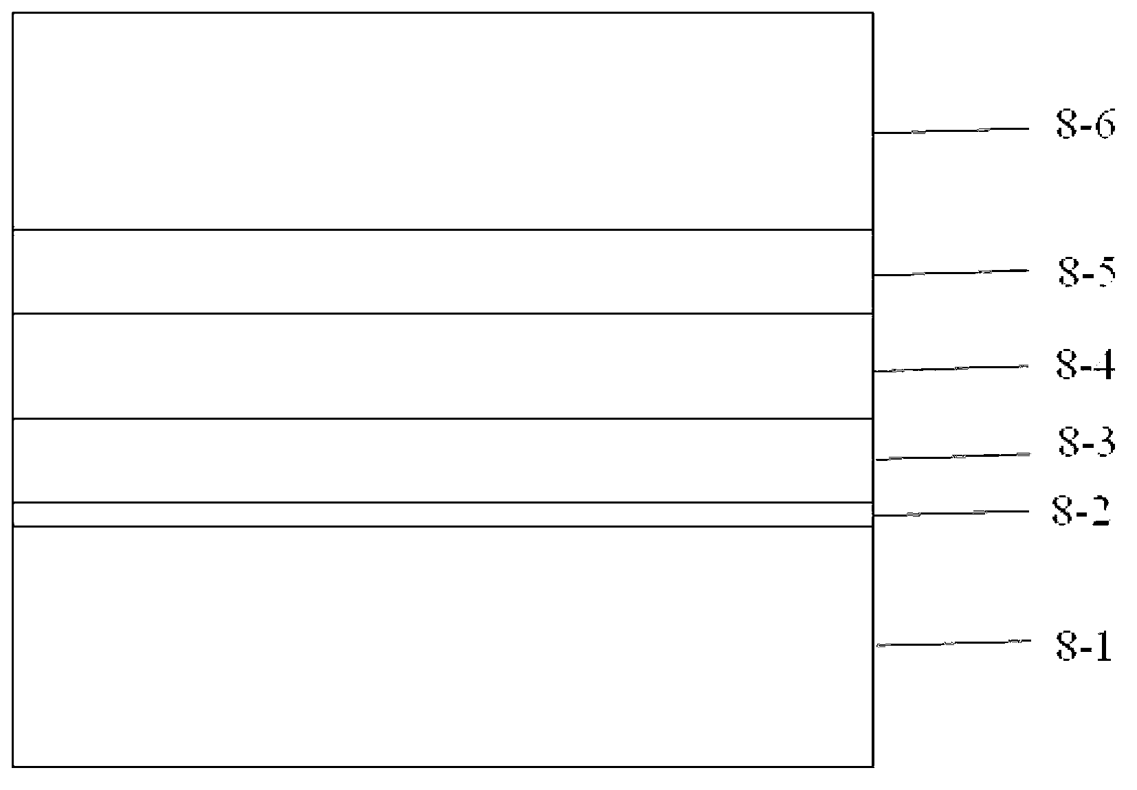
[0050] (1) Growth of red light-emitting diode epitaxial wafer 8: using metalorganic chemical vapor deposition (MOCVD) to sequentially grow Bragg reflector 8-2 and n-type aluminum gallium indium phosphorus layer 8-3 on GaAs substrate 8-1 , multi-quantum well layer 8-4, p-type aluminum gallium indium phosphide layer 8-5 and p-type GaP layer 8-6, prepared into a red light emitting diode epitaxial wafer;

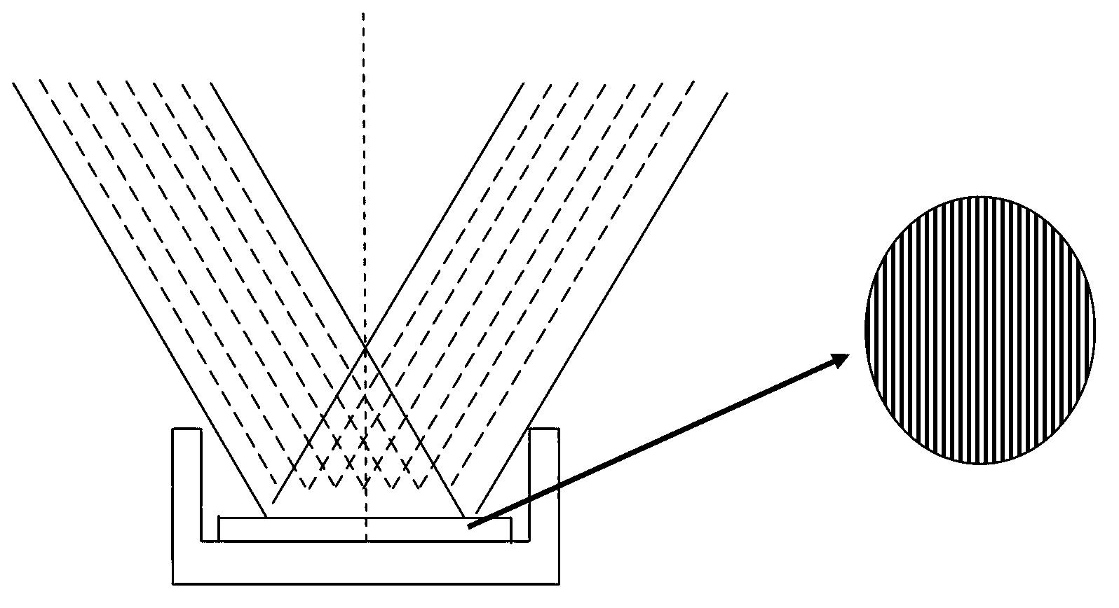
[0051] (2) Adjust the interference light path:

[0052] Put the red light-emitting diode epitaxial wafer 8 into a polytetrafluoroethylene flat-bottomed container 7, add deionized water to cover the surface to be etched (i.e. the p-type GaP layer) of the red light-emitting diode e...


PUM


Abstract

The invention relates to a method for implementing light emitting diode surface pattern preparation by using two-beam interference for assisting wet etching. The method includes: using a laser interference light path to irradiate a to-be-etched surface of a light emitting diode epitaxial wafer; adjusting the laser interference light path to form a light interference pattern on the to-be-etched surface of the light emitting diode epitaxial wafer; and subjecting the light emitting diode epitaxial wafer to light assisted wet etching by the aid of an existing wet etching method. Structures of different periods can be etched on the LED epitaxial wafer by adjusting angles of two incident laser beams. Compared with existing pattern preparation processes, the method has the advantages of simplicity in operation, low cost and acquisition of better surface patterns and microstructures.

Description

technical field [0001] The invention relates to a method for preparing surface patterns of light-emitting diodes by using double-beam interference-assisted wet etching, and belongs to the field of semiconductor optoelectronic materials and device preparation. Background technique [0002] In recent years, the application market of light-emitting diodes (LEDs) in solid-state lighting, large-area display screens, the automotive industry and new lighting fields has grown rapidly, and various countries are increasing research on light-emitting diodes. Driven by energy-saving requirements and commercial applications, light-emitting diode (LED) technology has been greatly developed, and it is considered to be the most promising new solid-state light source in the 21st century. [0003] For various technical indicators of light-emitting diodes, the most critical is its luminous efficiency. According to the structural characteristics of LED, there are two main ways to improve its l...

Claims


Application Information

Patent Timeline
Patent Type & Authority Applications(China)
IPC IPC(8): H01L33/22H01L33/00
Inventor 刘铎林贯军左志远冯兆斌张茜林晓煜徐现刚
Owner SHANDONG UNIV
Why Eureka
Try Eureka