


Quick Research
Generate reliable direction feasibility study reports for your R&D in just a few steps.

Technical Q&A
Discover and master advanced knowledge NOW. Basics, ideas, possibilities, all at once.

Find Solutions
As an expert in R&D theories, this can generate solutions to your technical problems instantly.

Evaluate Feasibility
Analyze your overall solution with one click, know your potential R&D risks in advance.

Monitor Landscape
Get weekly tech updates, stay abreast of the latest tech innovations and key insights.
Magnetic random access memory
A magnetic memory, magnetic layer technology, applied in static memory, digital memory information, information storage and other directions, can solve the problem of "unable to read data"
- Summary
- Abstract
- Description
- Claims
- Application Information
AI Technical Summary
Problems solved by technology
Method used
Image


Examples
no. 1 Embodiment approach )
[0031] (basic structure)
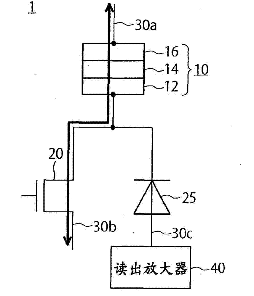
[0032] The basic structure of the memory cell of the MRAM of the first embodiment is shown in figure 1 middle. The memory cell 1 includes an MTJ element 10 , a selection transistor 20 , and a diode 25 . As the MTJ element 10 , for example, a perpendicular magnetization spin injection element composed of a leakage field adjustment layer / nonmagnetic layer / reference layer / tunnel barrier layer / recording layer / underground layer is used. Here, the notation "A / B" means that the A layer is located above the B layer. In addition, the MTJ element 10 only needs to include at least a reference layer whose magnetization direction is fixed perpendicular to the film surface, a recording layer whose magnetization direction is variable perpendicular to the film surface, and a tunnel barrier provided between the reference layer and the recording layer. layer. Here, the film surface refers to the upper surface of the magnetic layer.
[0033] As the selection trans...
no. 2 Embodiment approach )
[0056] The basic structure of the memory cell of the MRAM of the second embodiment is shown in Figure 9 middle. This memory cell 1 includes two MTJ elements 10 a and 10 b , one selection transistor 20 , and one diode 25 . The MTJ element 10a includes at least a recording layer 12a, a reference layer 16a, and a tunnel barrier layer 14a provided between the recording layer 12a and the reference layer 16a. In addition, the MTJ element 10b has at least a recording layer 12b, a reference layer 16b, and a tunnel barrier layer 14b provided between the recording layer 12b and the reference layer 16b. One terminal of the MTJ element 10a (that is, the electrode (not shown) on the side of the reference layer 16a) is connected to the first wiring 30a, and the other terminal (that is, the electrode (not shown) on the side of the recording layer 12a) is connected to one of the MTJ elements 10b. The terminal (an electrode (not shown) on the side of the recording layer 12 b ) is connected,...
PUM
 Abstract
Description
Claims
Application Information
 - R&D Engineer
- R&D Manager
- IP Professional
- Industry Leading Data Capabilities
- Powerful AI technology
- Patent DNA Extraction
Browse by: Latest US Patents, China's latest patents, Technical Efficacy Thesaurus, Application Domain, Technology Topic, Popular Technical Reports.
© 2024 PatSnap. All rights reserved.Legal|Privacy policy|Modern Slavery Act Transparency Statement|Sitemap|About US| Contact US: help@patsnap.com