Memory circuit
A storage circuit and circuit technology, which is applied in the field of storage circuits, can solve the problems of increasing circuit area, etc., and achieve the effects of reducing circuit area, power consumption, high-speed operation, and power consumption reduction
- Summary
- Abstract
- Description
- Claims
- Application Information
AI Technical Summary
Problems solved by technology
Method used
Image

Examples
Embodiment 1
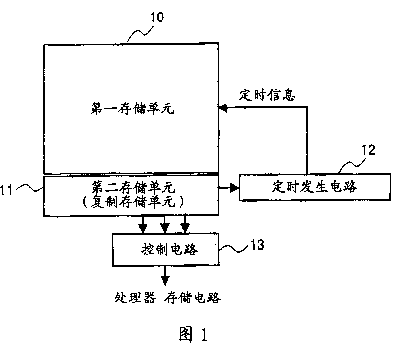
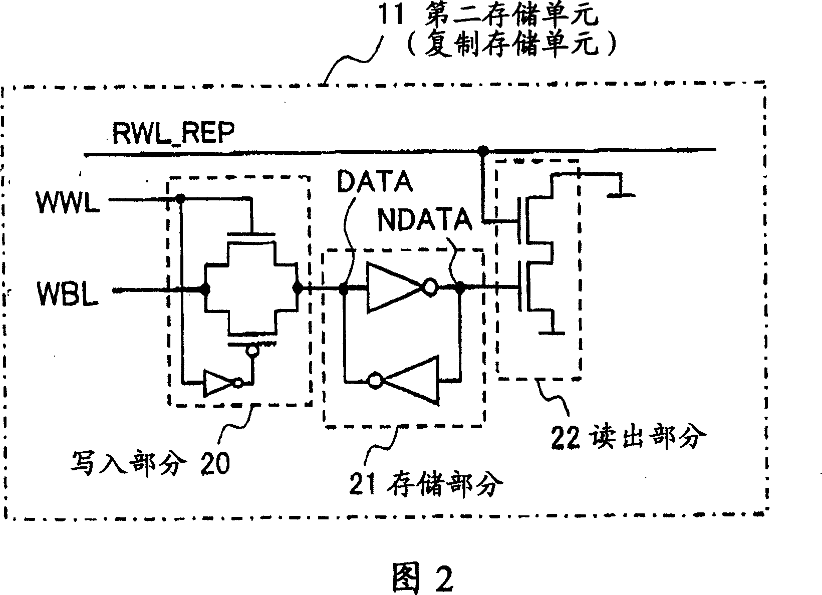
[0048] FIG. 1 is a structural block diagram of a storage circuit according to Embodiment 1 of the present invention. This block diagram shows a memory cell as a save hold circuit and its peripheral circuits. In FIG. 1, reference numeral "10" denotes a first storage unit, reference numeral "11" denotes a second storage unit, reference numeral "12" denotes a timing generation circuit, and reference numeral "13" denotes a control circuit. The first storage unit 10 is a single storage unit or a storage unit in an array configuration mapped to an address space accessible from the processor unit. The second memory unit 11 is not mapped to an address space, and is a memory unit single body or a memory unit having an array configuration having the same structure as the first memory unit 10 . The timing generating circuit 12 generates access timing for reading / writing of the first memory cell 10 with reference to information in the second memory cell 11 . The control circuit 13 has a...
Embodiment 2
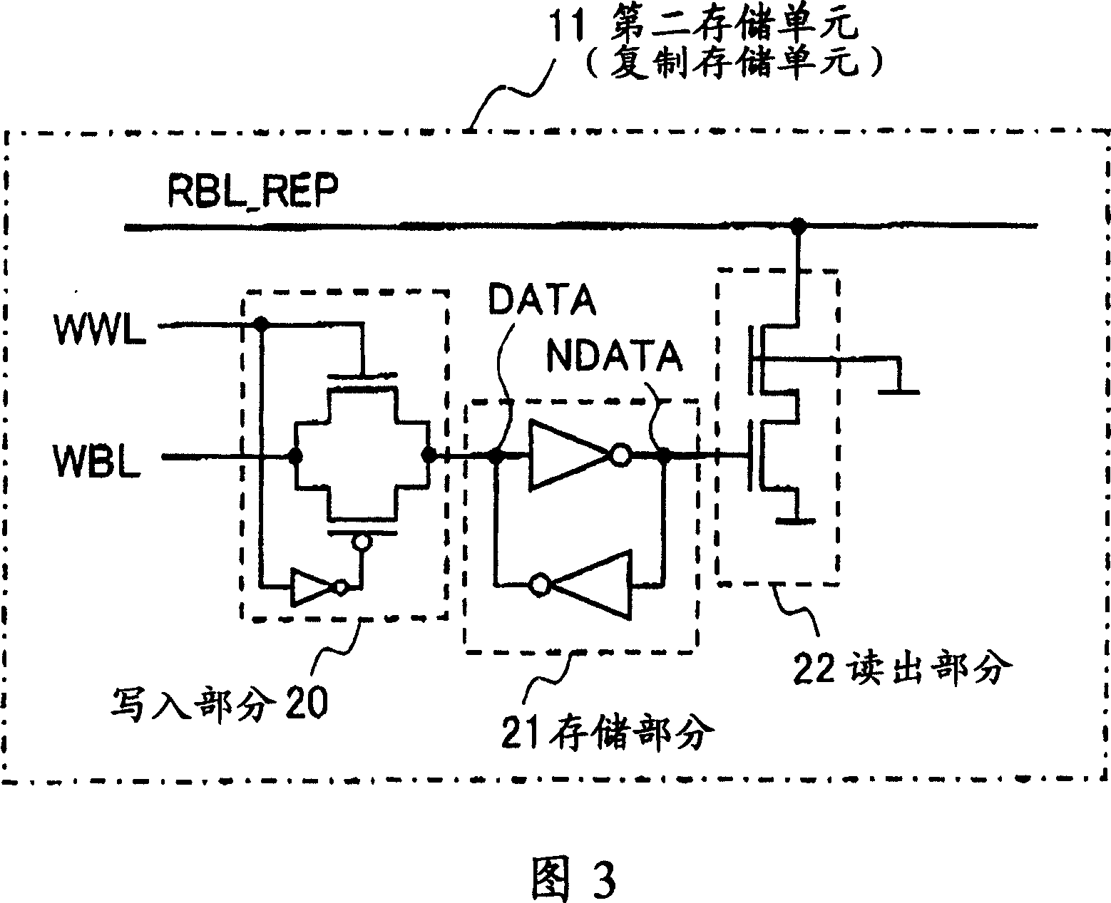
[0054] FIG. 4 is a structural block diagram of a storage circuit according to Embodiment 2 of the present invention. Unlike FIG. 1 , the second storage unit 11 is not used for timing generation, but for process compensation. In this memory circuit, the timing generating circuit 12 shown in FIG. 1 is not included. Conventionally, the output signal line of the second storage unit 11 is set to a suspended state or a fixed state, and the value held in the storage section (same as the storage section 21 of FIG. 2 ) of the second storage unit 11 is not used. In this embodiment, by connecting the output signal line to the control circuit 13, the value held in the aforementioned storage section can be used by the control circuit 13 (reference). Therefore, a holding circuit such as a flip-flop connected to the control circuit 13 is not required, so that the circuit area can be reduced.
[0055] The control circuit 13 can take various forms according to the controlled object and the c...
Embodiment 3
[0067] FIG. 5 is a structural block diagram of a storage circuit according to Embodiment 3 of the present invention. The storage circuit shown in this figure includes a first storage unit 10 , a second storage unit (duplicated storage unit) 11 , an address decoder 30 , an address buffer 31 and an IO circuit 32 . When the second storage unit 11 is used for process compensation purposes, peripheral circuits (eg, decoders) corresponding to the second storage unit 11 are not required. Therefore, as shown by the hatched area in FIG. 5, a vacant area 33 is generated in the area of the substrate on which the memory circuit is mounted close to the second memory cell 11. Referring to FIG. A further reduction in the circuit area can be achieved by arranging the control circuit 13 in said empty area 33 .
[0068] In the structure of FIG. 1, when the memory circuit is multi-ported, a readout portion of one or more ports is used in a signal line connecting the second memory cell 11 and ...
PUM
 Abstract
Description
Claims
Application Information
 - R&D
- Intellectual Property
- Life Sciences
- Materials
- Tech Scout
- Unparalleled Data Quality
- Higher Quality Content
- 60% Fewer Hallucinations
Browse by: Latest US Patents, China's latest patents, Technical Efficacy Thesaurus, Application Domain, Technology Topic, Popular Technical Reports.
© 2025 PatSnap. All rights reserved.Legal|Privacy policy|Modern Slavery Act Transparency Statement|Sitemap|About US| Contact US: help@patsnap.com