
Microencapsulated electrophoretic display with integrated driver

a micro-encapsulated and driver technology, applied in the association of printed circuit non-printed electric components, identification means, instruments, etc., can solve the problems of cost and reliability disadvantages of the approach, and achieve the effect of reducing costs, eliminating manufacturing steps, and joining steps

Inactive Publication Date: 2005-11-22
E INK CORPORATION
View PDF266 Cites 373 Cited by
  • Summary
  • Abstract
  • Description
  • Claims
  • Application Information

AI Technical Summary

Benefits of technology

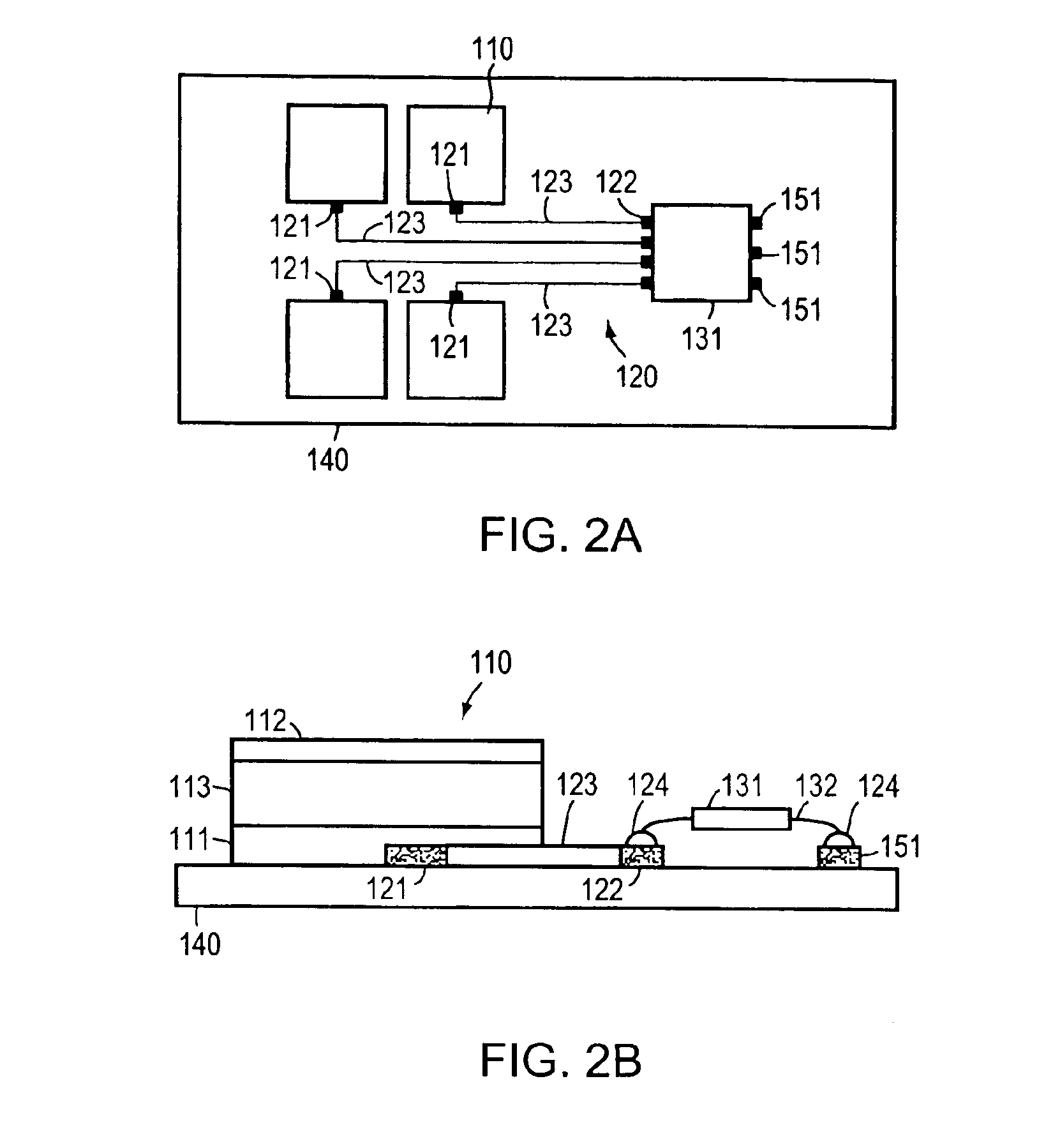
[0005]In a broad sense, the invention provides simpler, lower cost manufacturing methods and realization of the advantages of flexible displays through better use of flexible substrates. In one aspect, the invention provides a lower-cost, more flexible, and more useful display device through an electrophoretic display assembly and method of manufacturing the electrophoretic display assembly. In one embodiment, the display assembly comprises: a flexible substrate; an electrical connection formed on the flexible substrate; the electrical connection having first and second contact pads; an electrophoretic display element in electrical communication with the first contact pad; and a control circuit mounted on the flexible substrate and in electrical communication with the second contact pad.
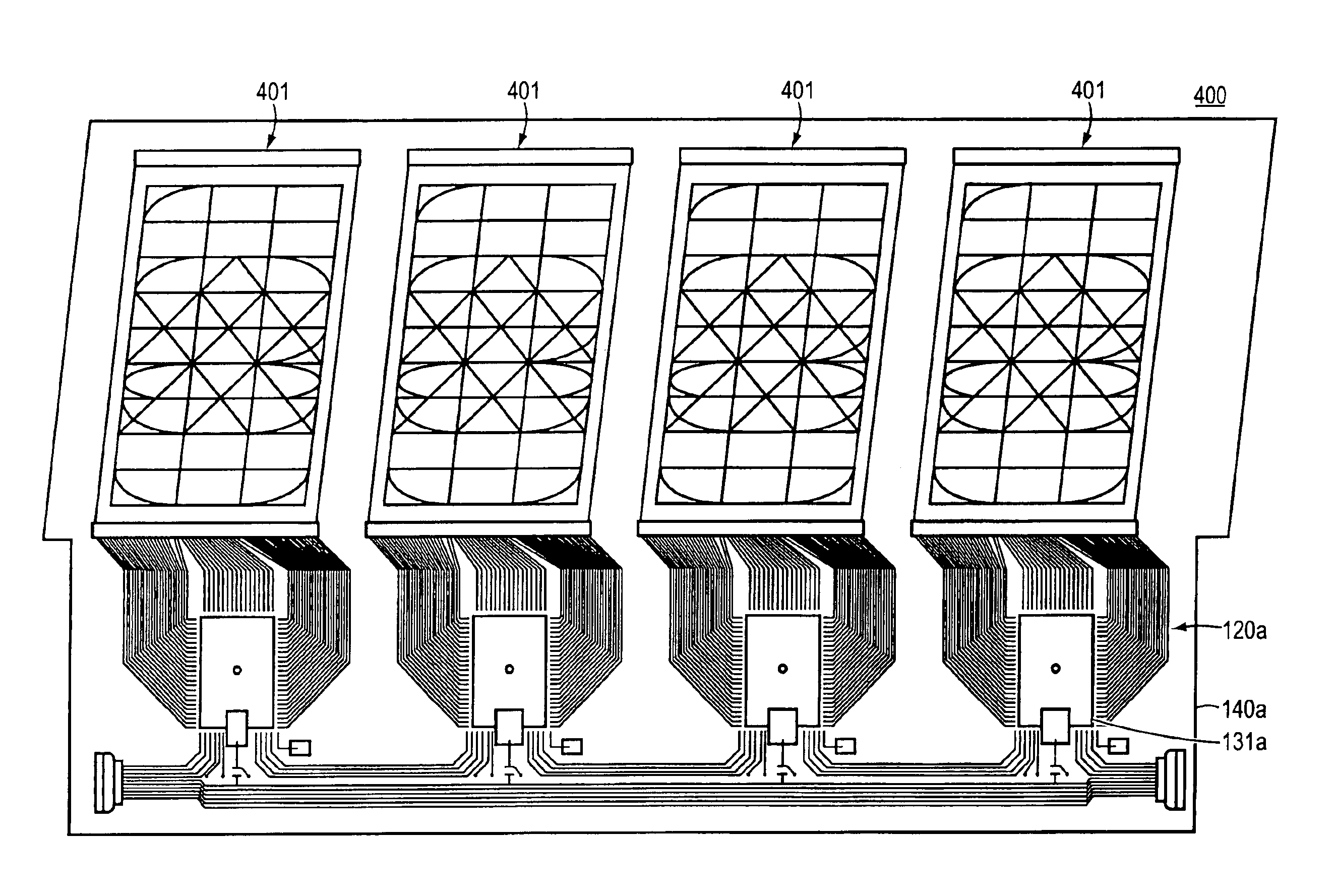
[0008]In contrast, the present invention, in one aspect, provides co-location of display elements and control circuitry on a shared, flexible substrate. This permits manufacturing of a flexible panel display. In one embodiment, use of an electrophoretic display medium, in particular an encapsulated electrophoretic display medium, leads to a flexible display that can be substantially flexed without substantial detrimental impact on the optical performance of the display medium.
[0009]Use of an encapsulated electrophoretic display medium further permits use of lower cost printing methods for deposition of the display medium. In a preferred embodiment, the display assembly provides for printing of electrical connections between display elements and control circuitry in a single printing step.
[0010]In one aspect, the invention eliminates the manufacturing steps that would be entailed in electrically and physically joining separate display medium substrate and control circuit substrate portions of a display. In the preferred embodiment of a common flexible substrate shared by the display medium and the control circuit, joining steps are eliminated, cost and yield are improved, and an overall more flexible structure is obtained.
[0011]The invention permits advantageous use of an electrophoretic display medium. An electrophoretic display has attributes of good brightness and contrast, wide viewing angles, state bistability, and low power consumption when compared with liquid crystal displays. In particular, use of an encapsulated (or “microencapsulated”) electrophoretic display medium provides advantages, such as the ability to print or coat the display medium on a wide variety of flexible or rigid substrates. Further, because the display medium can be printed (using a variety of methods), the display itself can be made less expensively.
[0012]A microencapsulated electrophoretic display medium is well suited to flexible display applications, since it can tolerate a high degree of flexing without substantial detrimental impact on its optical performance.

Problems solved by technology

This approach has cost and reliability disadvantages.

Method used


Image

  • Microencapsulated electrophoretic display with integrated driver
  • Microencapsulated electrophoretic display with integrated driver
  • Microencapsulated electrophoretic display with integrated driver

Examples


Embodiment Construction

[0025]In broad overview, the invention entails support of an electrophoretic display medium, control circuits, and electrical conductors on a common flexible substrate. This leads to manufacturing with lower cost of processing steps, and higher product yield. The resulting flexible display assembly has many advantageous uses, for example, in production of large area displays or display devices that can be flexed or rolled.

[0026]I. An Electrophoretic Display Assembly

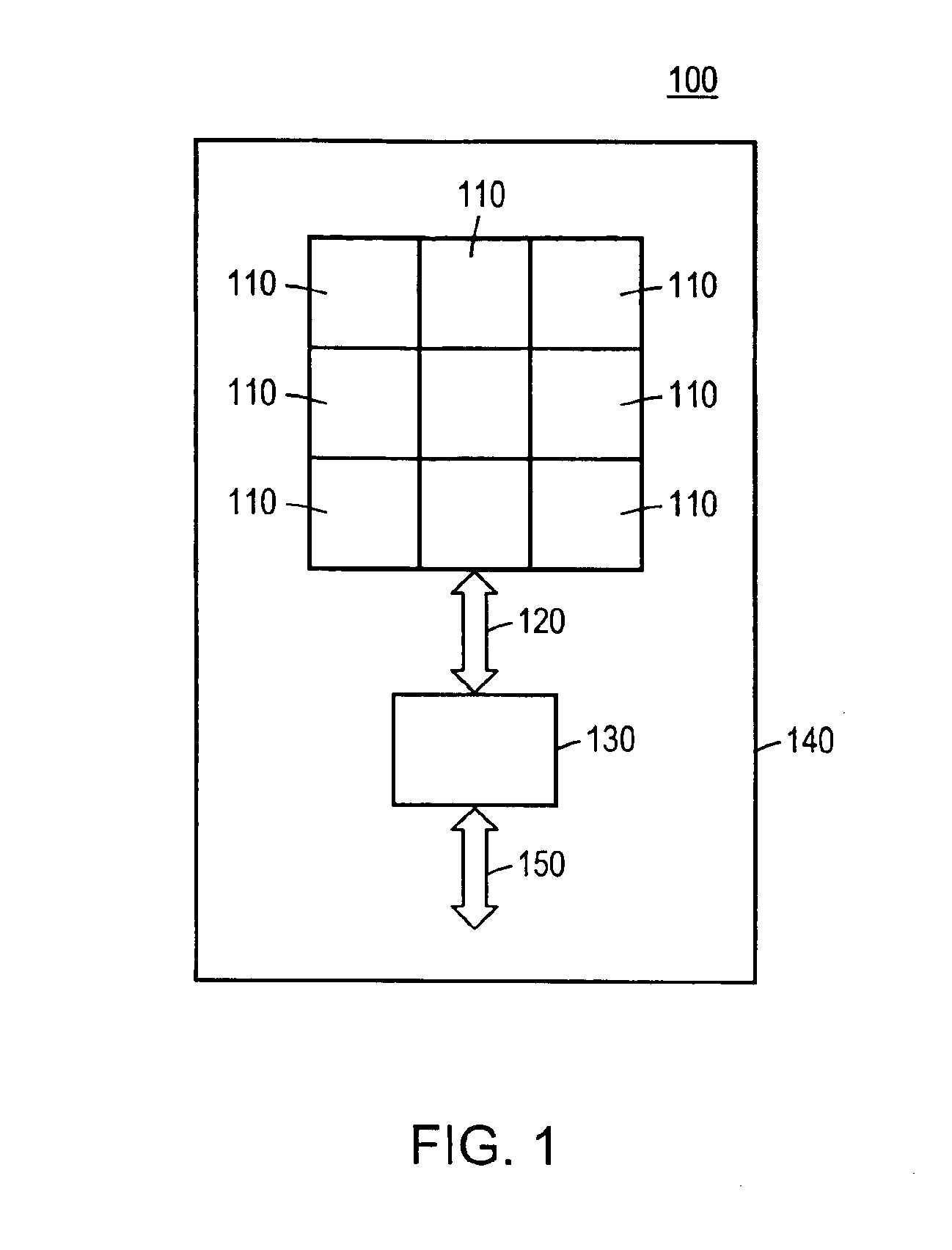
[0027]FIG. 1, in broad overview, depicts a schematic representation of an embodiment of an electrophoretic display assembly 100. The display assembly 100 comprises: electrophoretic display elements 110, each element 110 corresponding to a single pixel of the display assembly 100; a control circuit 130, the control circuit 130 in electrical communication with the display elements 110 via drive signal electrical connections 120, and in electrical communication with other components (not shown) either present on or off of a ...


PUM

PropertyMeasurementUnit
diameteraaaaaaaaaa
radiusaaaaaaaaaa
radiusaaaaaaaaaa

Abstract

A mounted display assembly comprises a flexible substrate that supports both display elements and control circuits. The display assembly generally comprises: an electrical connection formed on the flexible substrate, the electrical connection having first and second contact pads; a display element in electrical communication with the first contact pad; and a control circuit mounted on the flexible substrate and in electrical communication with the second contact pad. In a preferred embodiment, the display element comprises a microencapsulated electrophoretic display medium. In another preferred embodiment, printing processes are employed in manufacturing methods for the display assembly.

Description

TECHNICAL FIELD[0001]The invention relates generally to panel-type display devices and more particularly to flexible electrophoretic displays.BACKGROUND OF THE INVENTION[0002]Panel-type electronic display devices typically require a rigid circuit board mounted control circuit. For example, the liquid crystal displays found in laptop computers typically have several integrated circuits mounted on circuit boards, the circuit boards arranged around the liquid crystal portion of the panel. As panels of increasing size and resolution are developed, panels tend to require larger and heavier circuit boards in the manufacture of the display.[0003]Such printed circuit boards are expensive to manufacture and present the additional cost and complexity of physical and electrical interfacing with other display components. The added manufacturing steps required to connect the electrical conductors on the display medium portion of a display, e.g. the liquid crystal portion, with the electrical con...

Claims


Application Information

Patent Timeline
Patent Type & Authority Patents(United States)
IPC IPC(8): G02F1/01G02F1/167G09G3/16G02F1/16753G09F9/00H05K1/16H05K1/18
CPCG02F1/167G09G3/16H05K1/16H05K1/189G02F1/16753
Inventor ALBERT, JONATHAN D.GATES, HOLLY G.
Owner E INK CORPORATION
Learn More