Field emission display encapsulating method capable of realizing growth of CuO nano wire in encapsulating process
An encapsulation method and field emission technology, applied in the direction of cathode ray tube/electron beam tube, discharge tube, electrical components, etc., can solve the problems of emission characteristics decline and failure, and achieve the effect of simple production, avoiding damage and saving production cost.
- Summary
- Abstract
- Description
- Claims
- Application Information
AI Technical Summary
Problems solved by technology
Method used
Image
Examples
Embodiment 1
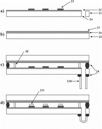
[0030] figure 2 Taking the diode structure device as an example, the process flow chart of making FED by one-time sintering is given. Such as figure 2 As shown in a), the cathode substrate 21 uses a glass substrate as a substrate, and an electrode layer 22 is prepared on the glass substrate. The electrode layer can be one or any combination of Cr, Al, Ti, ITO, and the thickness is about 200-600nm. Then use ultraviolet exposure or electron beam exposure to perform photolithography on the region where CuO nanowires need to be grown locally to obtain a photoresist pattern. Then prepare a layer of copper film on the photolithographic substrate by magnetron sputtering, thermal evaporation or electron beam evaporation. The thickness of the copper film is about 500nm~2μm. The power and time of the coating can be adjusted according to the thickness of the copper film. . The photoresist is removed by the stripping process, and the metal copper layer deposited directly on the glas...
Embodiment 2
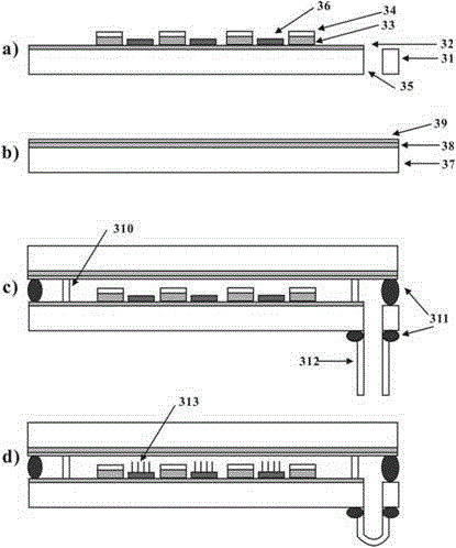
[0037] image 3 Taking the FED device with gate structure as an example, the specific implementation method of this patent is given. The structure of the cathode substrate is as image 3 As shown in a), the cathode substrate 31 adopts a glass substrate, on which a cathode electrode 32, an insulating layer 33, a grid 34, and an exhaust hole 35 are formed, and a copper film pattern 36 is prepared on the cathode electrode by using photolithography technology combined with coating technology. , the copper film thickness is about 500nm ~ 2μm.
[0038] image 3 b) is a schematic diagram of the anode substrate. The anode substrate 37 is a glass substrate on which a transparent conductive layer 38 and a phosphor layer 39 are fabricated.
[0039] Spacers 310 are evenly placed between the cathode substrate and the anode substrate to ensure insulation between cathode and anode and maintain a certain distance. Then the cathode plate and the anode plate are aligned and fixed with a clamp...
Embodiment 3
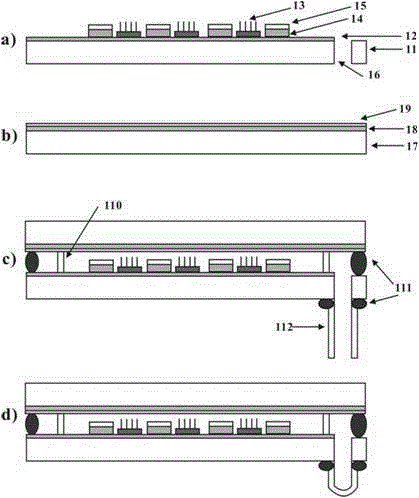
[0043] This embodiment takes a field emission display with a diode structure as an example, and provides a process for realizing the growth of CuO nanowires in the packaging process of the field emission display.
[0044] First, the glass substrate was ultrasonically cleaned with acetone, ethanol, and deionized water for 20 minutes, and then blown dry with nitrogen. A magnetron sputtering coater is used to coat a layer of ITO conductive layer on the glass substrate. The thickness of the ITO layer is about 400nm, and then uniformly coat photoresist on the conductive layer ITO, and then perform ultraviolet exposure through a mask. After exposure and development, a copper film is plated by magnetron sputtering. The thickness of the copper film is about 850nm. After coating, the photoresist is removed by a stripping process, leaving a copper film pattern on the substrate.
[0045] A spacer is placed between the cathode and anode substrates, aligned and fixed, and sealed with low-m...
PUM
| Property | Measurement | Unit |
|---|---|---|
| thickness | aaaaa | aaaaa |
| thickness | aaaaa | aaaaa |
| thickness | aaaaa | aaaaa |
Abstract
Description
Claims
Application Information
 - R&D
- Intellectual Property
- Life Sciences
- Materials
- Tech Scout
- Unparalleled Data Quality
- Higher Quality Content
- 60% Fewer Hallucinations
Browse by: Latest US Patents, China's latest patents, Technical Efficacy Thesaurus, Application Domain, Technology Topic, Popular Technical Reports.
© 2025 PatSnap. All rights reserved.Legal|Privacy policy|Modern Slavery Act Transparency Statement|Sitemap|About US| Contact US: help@patsnap.com


