Lens for achieving curved-surface-to-plane super-resolution demagnification imaging photo-etching
A super-resolution and curved surface technology, applied in the direction of lens, microlithography exposure equipment, optics, etc., can solve the problems of limited structure and low quality of lithography imaging, achieve the effect of reducing the size of graphics and overcoming the low quality of imaging
- Summary
- Abstract
- Description
- Claims
- Application Information
AI Technical Summary
Problems solved by technology
Method used
Image
Examples
specific Embodiment 1
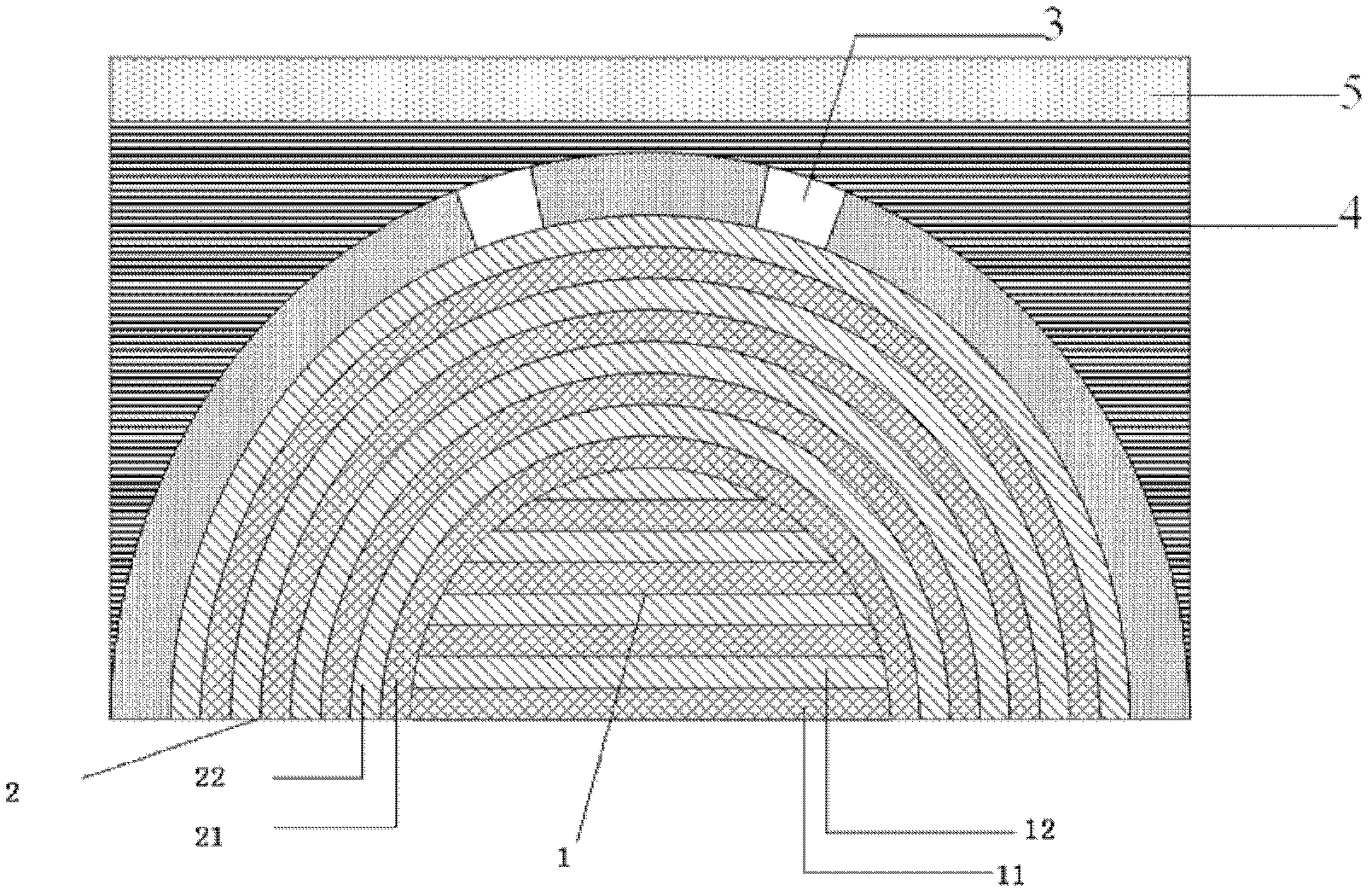
[0030] According to the present invention, a lens for realizing super-resolution zooming imaging lithography from a curved surface to a plane and a manufacturing method thereof, the specific implementation steps are as follows:
[0031] (1) The designed planar multilayer film structure is composed of a metal Ag layer and a dielectric SiO 2 Layer composition, first vapor-deposit Ag layer, then vapor-deposit SiO 2 Layers, alternating 5 groups of 10 layers. The thickness of each layer is 10nm, a total of 100nm;
[0032] (2) The designed curved multilayer film structure is obtained by sputtering. Co-deposition of 10 groups of 20 layers, first depositing Ag and then SiO 2 , alternately depositing 10 groups. Control the thickness of each layer to be 20nm, total thickness=400nm;
[0033] (3) The designed metal mask structure is obtained by magnetron sputtering coating, the metal to be coated is chromium film, the coating power is 700W, and the film thickness is 50nm. Slit the c...
specific Embodiment 2
[0036] Another kind of lens and its manufacturing method for realizing surface-to-plane super-resolution reduction imaging lithography, its specific implementation steps are as follows:
[0037] (1) The designed planar multilayer film structure includes metal layers and dielectric layers. Using the sputtering method, the metal Ag layer is sputtered first, and then the dielectric SiO 2 Layers, alternating 8 groups of 16 layers. The thickness of each layer is 20nm, a total of 320nm, and the surface roughness is required to be ≤2nm;
[0038] (2) The designed curved multilayer film structure is obtained by vapor deposition. A total of 15 groups of 30 layers were evaporated, first the metal Ag layer was evaporated and then SiO 2 Layers, alternately vapor-deposited 15 groups. Control the thickness of each layer to be 20nm, total thickness=600nm;
[0039] (3) The designed metal mask structure is obtained by magnetron sputtering coating, and the coated metal is a chromium film wi...
specific Embodiment 3
[0042] Another kind of lens and its manufacturing method for realizing surface-to-plane super-resolution reduction imaging lithography, its specific implementation steps are as follows:
[0043] (1) The designed planar multilayer film structure is composed of a metal Ag layer and a dielectric SiO 2 Layer composition, depositing Ag layer first, then SiO 2 Layers, alternate 10 groups of 20 layers. The thickness of each layer is 30nm, a total of 600nm;
[0044] (2) The designed curved multilayer film structure is prepared by evaporation. A total of 20 groups of 40 layers were evaporated, first evaporated Ag and then SiO 2 , Alternately evaporate 20 groups. Control the thickness of each layer to be 30nm, total thickness=1200nm;
[0045] (3) The designed metal mask structure is obtained by vapor-deposited film, and the plated metal is a chromium film with a film thickness of 150nm. Make a slit on the chromium film so that the slit width is 150nm and the slit spacing is 500nm;...
PUM
| Property | Measurement | Unit |
|---|---|---|
| thickness | aaaaa | aaaaa |
| power | aaaaa | aaaaa |
| thickness | aaaaa | aaaaa |
Abstract
Description
Claims
Application Information
 - R&D
- Intellectual Property
- Life Sciences
- Materials
- Tech Scout
- Unparalleled Data Quality
- Higher Quality Content
- 60% Fewer Hallucinations
Browse by: Latest US Patents, China's latest patents, Technical Efficacy Thesaurus, Application Domain, Technology Topic, Popular Technical Reports.
© 2025 PatSnap. All rights reserved.Legal|Privacy policy|Modern Slavery Act Transparency Statement|Sitemap|About US| Contact US: help@patsnap.com


