Preparation method of self-supporting multiferroics composite film
A composite thin film, multiferroic technology, applied in the manufacture/processing of electromagnetic devices, material selection, etc., can solve the problem of thickness, generally between a few micrometers to several hundreds of micrometers, is not easy to miniaturize devices, and has poor operability. Good and other problems, to achieve the effect of low cost, easy miniaturization, simple and controllable process
- Summary
- Abstract
- Description
- Claims
- Application Information
AI Technical Summary
Problems solved by technology
Method used
Image
Examples
Embodiment 1
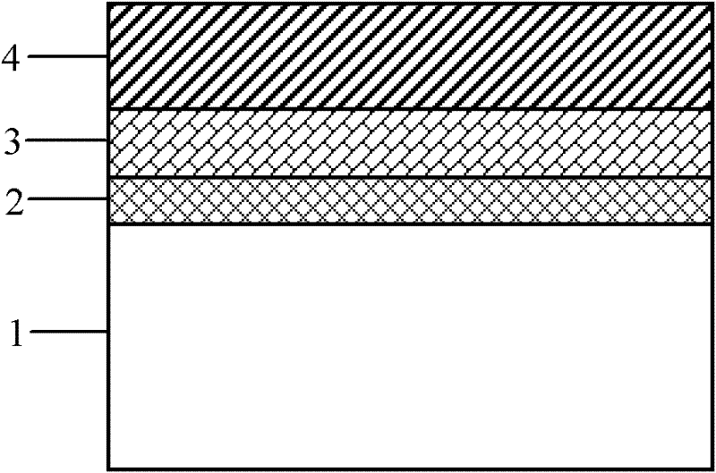
[0030] Embodiment 1: adopt platinum-coated silicon chip, the structure of this platinum-coated silicon chip is as figure 2 As shown, it is composed of a silicon layer 1, an intermediate layer and a platinum thin film layer 4. The intermediate layer is a composite layer composed of a silicon dioxide layer 2 and a titanium layer 3. The thickness of the silicon layer 1 is 500 μm, and the silicon dioxide The thickness of layer 2 is 5nm, the thickness of titanium layer 3 is 50nm, and the thickness of platinum film layer 4 is 200nm; 2 Put into the small piece of hydrofluoric acid (HF) aqueous solution that mass percent concentration is 10% and etch for 7 hours, make the silicon dioxide layer 2 and titanium layer 3 of platinum-plated silicon chip react with hydrofluoric acid, platinum thin film layer 4. The silicon wafer layer 1 falls off by itself and floats on the surface of the solution to obtain a self-supporting platinum film; then use a clean silicon wafer to pick up the self-...
Embodiment 2
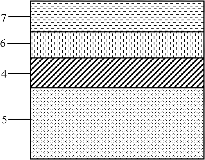
[0031]Embodiment 2: the preparation method of self-supporting multiferroic thin film in this embodiment is basically the same as embodiment 1, and difference is to adopt magnetron sputtering method to deposit iron thin film on ferroelectric layer thin film 6 as ferromagnetic layer thin film 7. The sputtering conditions are: argon atmosphere, argon flow rate 50sccm, sputtering pressure 1Pa, sputtering power 20W, sputtering time 20min, the obtained structure is as follows image 3 The shown self-supporting multiferroic composite film.
PUM
| Property | Measurement | Unit |
|---|---|---|
| thickness | aaaaa | aaaaa |
| thickness | aaaaa | aaaaa |
| thickness | aaaaa | aaaaa |
Abstract
Description
Claims
Application Information
 - R&D
- Intellectual Property
- Life Sciences
- Materials
- Tech Scout
- Unparalleled Data Quality
- Higher Quality Content
- 60% Fewer Hallucinations
Browse by: Latest US Patents, China's latest patents, Technical Efficacy Thesaurus, Application Domain, Technology Topic, Popular Technical Reports.
© 2025 PatSnap. All rights reserved.Legal|Privacy policy|Modern Slavery Act Transparency Statement|Sitemap|About US| Contact US: help@patsnap.com


