Thermally reactive resist material, laminated body for thermal lithography using the material, and mold manufacturing method using the material and the laminated body
A thermal reaction and resist technology, which is applied in the field of laminates for thermal lithography, can solve the problems of low precision pattern processing, loss of uniformity, difficulty in controlling pattern size, etc.
- Summary
- Abstract
- Description
- Claims
- Application Information
AI Technical Summary
Problems solved by technology
Method used
Image


Examples
Embodiment 1
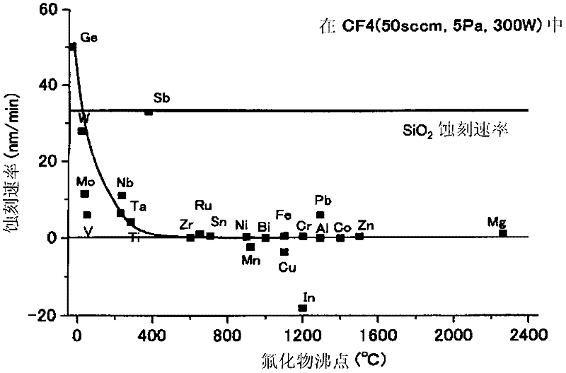
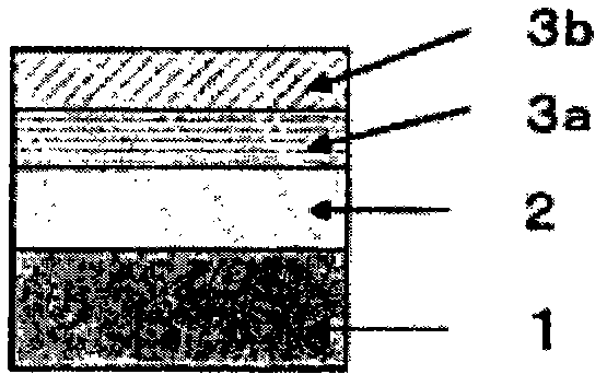
[0159] Select Cr 1-x o x , Nb 1-x o x 、 Ta 1-x o x 、Ti 1-x o x As a transition metal heat-reactive resist material. In addition, the etch layer chooses SiO 2 .
[0160] First, a film of 350 nm was formed under the conditions in Table 3 below on a glass flat substrate of 50 mmφ by a sputtering method using a SiO2 target. Next, a Cr target of 40 nm was formed under the conditions in Table 3 using a Cr target 1-x o x membrane. For heat reactive resist material Nb 1-x o x 、 Ta 1-x o x 、Ti 1-x o x , and also the first SiO with a film thickness of 350nm 2 Film formation, after that, under the conditions in Table 3, Nb 1-x o x 、 Ta 1-x o x 、Ti 1-x o x film forming.
[0161] [table 3]
[0162]
[0163] Table 3 shows the X values obtained by analyzing the metal-to-oxide ratios of the deposited heat-reactive resist materials by fluorescent X-rays. In addition, under the same conditions as above, only the respective heat-reactive resist materials were form...
Embodiment 2
[0176] Select Sn 1-x o x , Pb 1-x o x As a heat-reactive resist material for group XII-XV elements. Same as embodiment 1, these heat-reactive resists are also under the conditions shown in table 3, respectively on SiO with a film thickness of 350nm 2 film-on-film.
[0177] The heat-reactive resist after stacking was analyzed by fluorescent X-ray, and the X value obtained is shown in Table 3. In addition, under the same conditions as above, only the respective heat-reactive resist materials were formed into a film, and XRD analysis was performed, and all the materials were amorphous in which no clear diffraction pattern could be obtained. As in Example 1, the above-mentioned film-formed resist layer was exposed.
[0178] Next, the heat-reactive resist exposed by the above-mentioned exposure machine is developed. About image development also, it carried out under the conditions shown in Table 4 similarly to Example 1.
[0179] The surface shape and cross-sectional shape ...
Embodiment 3
[0183] In addition to choosing Cr 1-x o x As a transition metal heat-reactive resist material, Te 1-x o x Film formation, exposure, and image development were performed in the same manner as in Example 1 except for the etching layer. Te 1-x o x The film-forming conditions are shown in Table 3.
[0184] Next, using the heat-reactive resist as a mask, Te 1-x o x of etching. Dry etching using CF 4 As an etching gas, it carried out under the conditions of 5 Pa of processing gas pressure, 400 W of processing electric power, and 20 minutes of processing time. After etching, SEM (scanning electron microscope) was used to observe its surface shape and cross-sectional shape again, and the etching layer depth (nm) and resist film thickness (nm) constituting the aspect ratio shown in Table 4 were observed, and the etching layer reflected While the width shape of the mask is patterned, the mask maintains its shape without being etched.
[0185] Only the heat-reactive resist is ...
PUM
| Property | Measurement | Unit |
|---|---|---|
| boiling point | aaaaa | aaaaa |
| wavelength | aaaaa | aaaaa |
| boiling point | aaaaa | aaaaa |
Abstract
Description
Claims
Application Information
 - R&D
- Intellectual Property
- Life Sciences
- Materials
- Tech Scout
- Unparalleled Data Quality
- Higher Quality Content
- 60% Fewer Hallucinations
Browse by: Latest US Patents, China's latest patents, Technical Efficacy Thesaurus, Application Domain, Technology Topic, Popular Technical Reports.
© 2025 PatSnap. All rights reserved.Legal|Privacy policy|Modern Slavery Act Transparency Statement|Sitemap|About US| Contact US: help@patsnap.com