Method for manufacturing bipolar transistor

A technology of bipolar transistors and manufacturing methods, applied in semiconductor/solid-state device manufacturing, semiconductor devices, electrical components, etc., capable of solving problems such as optimization of bipolar transistors

Active Publication Date: 2011-05-25
CSMC TECH FAB2 CO LTD
View PDF0 Cites 1 Cited by
  • Summary
  • Abstract
  • Description
  • Claims
  • Application Information

AI Technical Summary

Problems solved by technology

[0005] In view of this, it is necessary to address the shortcomings of the above-mentioned high-temperature thermal annealing method for repairing lattice surface defects that can not optimize the performance of bipolar transistors without affecting the performance of other devices, and provide a method that can improve bipolar transistors. Method for manufacturing bipolar transistor with current gain

Method used


Image

  • Method for manufacturing bipolar transistor
  • Method for manufacturing bipolar transistor
  • Method for manufacturing bipolar transistor

Examples


Embodiment Construction

[0026] The specific embodiments of the present invention will be described in detail below in conjunction with the accompanying drawings.

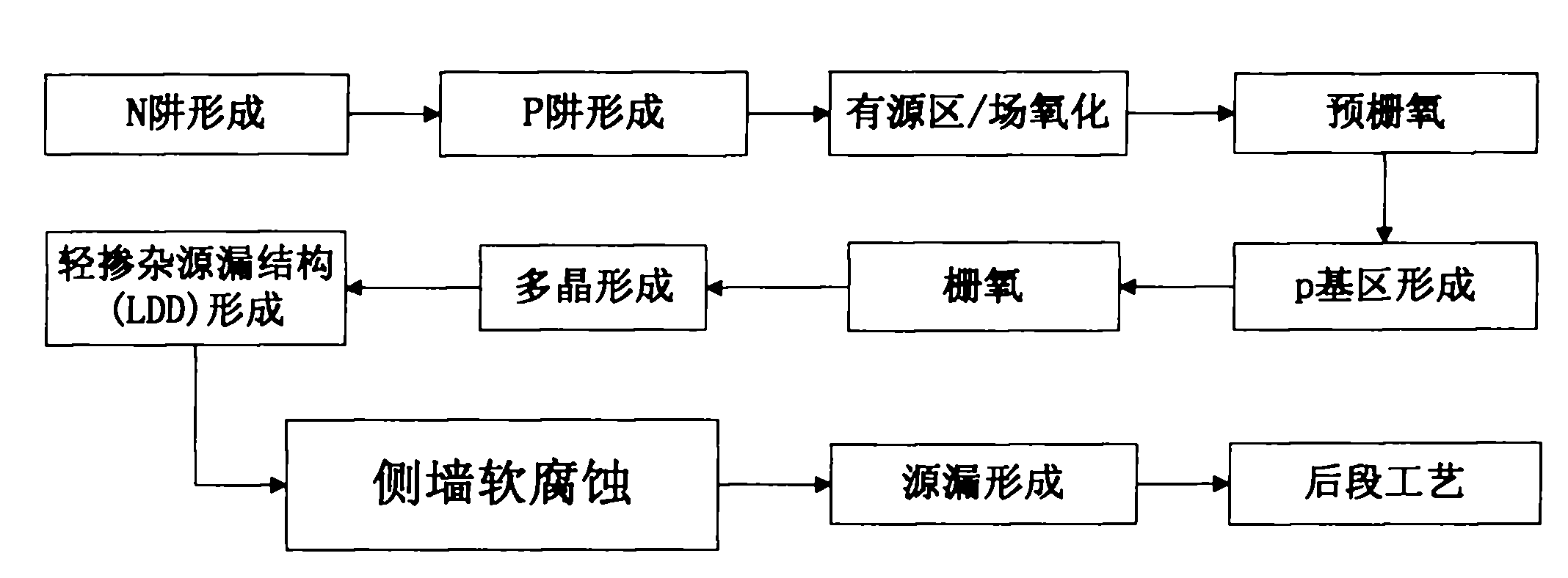
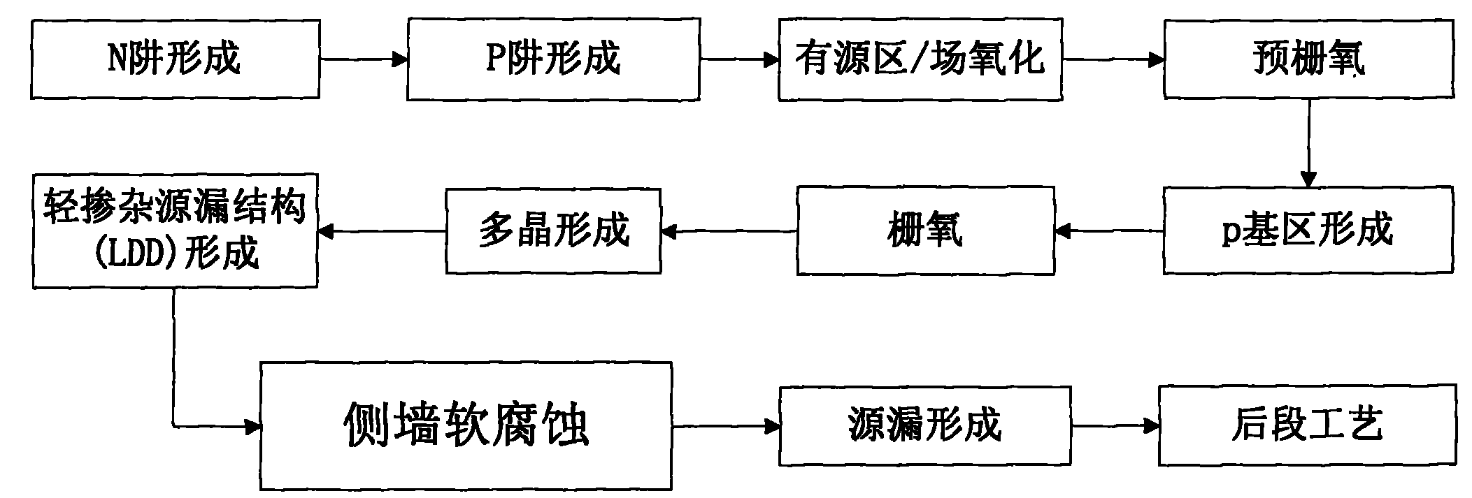
[0027] figure 1 It is a schematic diagram of a manufacturing method of a bipolar transistor according to a preferred embodiment of the present invention. Including the following steps:

[0028] N well formation: the wafer undergoes a photolithography process (photoresist spin coating, photoresist exposure, development, and inspection), and phosphorus ion implantation forms the well region that constitutes the PMOS and the collector that constitutes the bipolar transistor.

[0029] P well formation: The wafer is also formed by photolithography and boron ion implantation to form the well region of NMOS.

[0030] Active area / field oxidation: After the active area photolithography process, after the hard mask is etched away, a field oxide layer is formed by a high temperature and wet oxidation process.

[0031] Pre-gate oxide: After the waf...


PUM


Abstract

The invention relates to a method for manufacturing a bipolar transistor, which comprises the following steps of: forming a complementary metal oxide semiconductor (CMOS) gate; performing low pressure deposition to form a tetraethoxysilane layer on the gate; performing a sidewall soft corrosion process, etching the tetraethoxysilane layer and repairing silicon wafer surface defects caused by the etching; and forming a CMOS source and a CMOS drain. In the method, a film layer forming a sidewall is etched and the silicon wafer surface defects caused by the etching are repaired, so a current workspace is increased and the current gain of the vertical NPN bipolar transistor is greatly improved.

Description

【Technical field】 [0001] The invention relates to a manufacturing method of a bipolar transistor, in particular to a manufacturing method capable of improving the current gain of the bipolar transistor. 【Background technique】 [0002] In the traditional submicron analog complementary metal-oxide semiconductor (Analog CMOS) process, the base region of the bipolar transistor (Bipolar) is formed by the P-type base layer (P-base), and the source-drain injection layer increases the bipolar transistor accordingly. The emitter is implanted, and the collector of the bipolar transistor is formed by the substrate, thereby forming a vertical NPN (N+ / P-base / N-Well) bipolar transistor. [0003] During the process, the formation process of the sidewall (Spacer) is before the formation of the CMOS source and drain (simultaneously implanting the emitter of the bipolar transistor), so the surface of the bipolar transistor device will be strongly bombarded by the plasma in the sidewall etchin...

Claims


Application Information

Patent Timeline
Patent Type & Authority Applications(China)
IPC IPC(8): H01L21/331H01L21/8238H01L21/28
Inventor 胡金节肖中强陈正培李月影赵英翰吴孝嘉
Owner CSMC TECH FAB2 CO LTD
Why Eureka
Try Eureka