GaN-based hot electron transistor on self-supporting substrate and preparation method of GaN-based hot electron transistor

A technology of self-supporting substrates and thermal electrons, applied in semiconductor/solid-state device manufacturing, circuits, electrical components, etc., can solve the problems of failure to realize common emitter operation of devices, achieve large collector current, good working performance, The effect of high breakdown field strength

Pending Publication Date: 2021-12-03
XIDIAN UNIV
View PDF2 Cites 0 Cited by
  • Summary
  • Abstract
  • Description
  • Claims
  • Application Information

AI Technical Summary

Problems solved by technology

The report confirmed that the current injection mechanism is a thermal emission mechanism, and finally achieved a common base current gain of 0.97 to 0.98, but failed to realize the common emitter operation of the device

Method used


Image

  • GaN-based hot electron transistor on self-supporting substrate and preparation method of GaN-based hot electron transistor
  • GaN-based hot electron transistor on self-supporting substrate and preparation method of GaN-based hot electron transistor
  • GaN-based hot electron transistor on self-supporting substrate and preparation method of GaN-based hot electron transistor

Examples


Embodiment 1

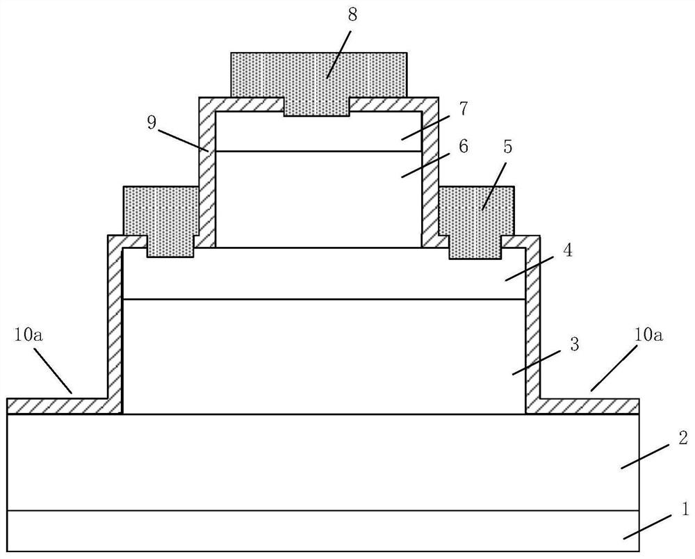
[0042] See figure 1 and figure 2 , figure 1 A schematic structural diagram of a GaN-based thermionic transistor on a self-supporting substrate provided by an embodiment of the present invention, figure 2 A schematic structural diagram of another GaN-based thermionic transistor on a self-supporting substrate provided in an embodiment of the present invention.

[0043] The GaN-based thermionic transistor device is a unipolar vertical structure, including a collector 1, a GaN self-supporting substrate 2, Al y Ga 1-y N collector 3, GaN base 4, base 5, Al x Ga 1-x N emitter region 6 , n+GaN cap layer 7 , emitter 8 and passivation layer 9 .

[0044] Among them, collector 1, GaN free-standing substrate 2, Al y Ga 1-y N collector region 3, GaN base region 4, Al x Ga 1-x The N emitter region 6 and the n+GaN cap layer 7 are stacked in sequence, and the Al x Ga 1-x The N emitter region 6 and the n+GaN cap layer 7 form a mesa structure; the passivation layer 9 is located in ...

Embodiment 2

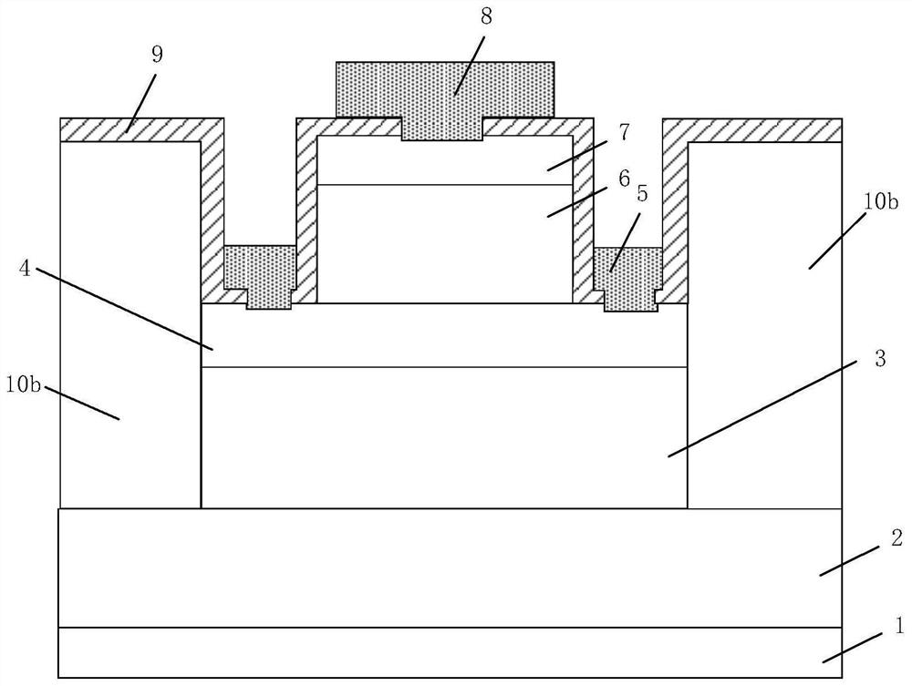
[0059] On the basis of Example 1, please refer to Figure 4 , Figure 4 A schematic flowchart of a method for fabricating a GaN-based thermionic transistor on a self-supporting substrate provided in an embodiment of the present invention.

[0060] In this embodiment, GaN self-supporting substrates 2 and Al that are stacked sequentially from bottom to top are selected.y Ga 1-y N collector region 3, GaN base region 4, Al x Ga 1-x The structure of the N emitter region 6 and the n+GaN cap layer 7 serves as an epitaxial substrate.

[0061] Specifically, the preparation method of the GaN-based thermionic transistor on the self-supporting substrate comprises the steps of:

[0062] S1. Fabricating an electrical isolation structure for the active region of the device on an epitaxial substrate.

[0063] S11 , photolithography the electrical isolation region of the active region on the n+GaN cap layer 7 .

[0064] S12, using the inductively coupled plasma etching process ICP to seq...

Embodiment 3

[0085] On the basis of Embodiment 1 and Embodiment 2, this embodiment provides a GaN-based thermionic transistor on a self-supporting substrate and a preparation method thereof, please refer to Figures 5a-5g , Figures 5a-5g A process schematic diagram of a method for fabricating a GaN-based thermionic transistor on a self-supporting substrate provided in an embodiment of the present invention.

[0086] The GaN-based thermionic transistor includes a collector 1, a GaN free-standing substrate 2, Al y Ga 1-y N collector 3, GaN base 4, base 5, Al x Ga 1-x N emitter 6, n+GaN cap layer 7, emitter 8 and passivation layer 9, such as Figure 5a shown. For the specific structure of the device, please refer to Embodiment 1, which will not be repeated in this embodiment.

[0087] Specifically, the GaN-based thermionic transistor is selected from the collector electrode 1, the GaN self-supporting substrate 2, the Al y Ga 1-y N collector region 3, GaN base region 4, Al x Ga 1-x ...


PUM

PropertyMeasurementUnit
thicknessaaaaaaaaaa
thicknessaaaaaaaaaa
thicknessaaaaaaaaaa

Abstract

The invention relates to a GaN-based hot electron transistor on a self-supporting substrate and a preparation method of the GaN-based hot electron transistor. The GaN-based hot electron transistor comprises a collector electrode, an n + GaN self-supporting substrate, an AlyGa1-yN collector region, a GaN base region, a base electrode, an AlxGa1-xN emitter region, an n+ GaN cap layer, an emitter electrode and a passivation layer, wherein the collector electrode, the n + GaN self-supporting substrate, the AlyGa1-yN collector region, the GaN base region, the AlxGa1-x N emitter region and the n+ GaN cap layer are stacked in sequence, the AlxGa1-xN emitter region and the n+ GaN cap layer form a mesa structure, and the passivation layer is located on the surfaces of an electrical isolation structure, the GaN base region, the AlxGa1-xNemitter region and the n+ GaN cap layer; the upper end of the base electrode is positioned on the surface of the passivation layer on the GaN base region and is in contact with the passivation layer on the side surface of the mesa structure, and the lower end of the base electrode is positioned in the passivation layer and is in contact with the GaN base region; and the upper end of the emitter is located on the surface of the passivation layer on the mesa structure, and the lower end of the emitter is located in the passivation layer and makes contact with the n+ GaN cap layer. The GaN-based hot electron transistor has the advantages of large collector current, high breakdown field strength, low epitaxial material defect density and the like, and can exert better working performance.

Description

technical field [0001] The invention belongs to the technical field of semiconductor devices, and in particular relates to a GaN-based thermionic transistor on a self-supporting substrate and a preparation method thereof. Background technique [0002] GaN material has become an important material for the development of high-temperature and high-power electronic devices and high-frequency microwave devices because of its excellent characteristics such as large band gap, high breakdown field strength, high electron saturation velocity, and high thermal conductivity. [0003] At present, the field of high-frequency and high-power devices is dominated by laterally structured high electron mobility transistors (HEMTs). It uses the high concentration two-dimensional electron gas (2DEG) generated by the polarization effect at the AlGaN / GaN heterojunction interface to work. Due to its high carrier mobility and high current density, HEMT devices can be used in high frequency The fie...

Claims


Application Information

Patent Timeline
Patent Type & Authority Applications(China)
IPC IPC(8): H01L29/76H01L29/207H01L29/205H01L29/20H01L21/335
CPCH01L29/7606H01L29/66939H01L29/2003H01L29/205H01L29/207
Inventor 马晓华祝杰杰张颖聪王鹏飞宓珉瀚郝跃
Owner XIDIAN UNIV
Why Eureka
Try Eureka