Eureka AIR delivers breakthrough ideas for toughest innovation challenges, trusted by R&D personnel around the world.

Improved NiO-based resistive random access memory (RRAM) and manufacturing method thereof

A technology of resistive random access and random access memory, applied in the field of memory, can solve the problems of difficulty in reducing the writing voltage, reducing the number of charges, and deteriorating reliability, achieving stable resistance value, avoiding erasing and writing failure, and improving stability and reliability. sexual effect

Inactive Publication Date: 2011-04-06
FUDAN UNIV
View PDF5 Cites 7 Cited by
  • Summary
  • Abstract
  • Description
  • Claims
  • Application Information

AI Technical Summary

Problems solved by technology

[0002] Non-volatile memory technology is currently a research hotspot in the field of information storage technology. With the further shrinking of the feature size of semiconductor devices, the amount of charge stored in traditional floating gate transistor memory is reduced, the write voltage is difficult to drop, and the reliability is also changing. Poor, so the development of new non-volatile memory becomes very important

Method used


Image

  • Improved NiO-based resistive random access memory (RRAM) and manufacturing method thereof
  • Improved NiO-based resistive random access memory (RRAM) and manufacturing method thereof
  • Improved NiO-based resistive random access memory (RRAM) and manufacturing method thereof

Examples


Embodiment Construction

[0026] Below in conjunction with accompanying drawing and specific embodiment the present invention is described in further detail:

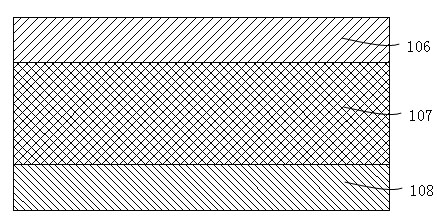
[0027] The silicon dioxide dielectric layer 110 is grown on the monocrystalline silicon 100 layer by means of thermal oxidation or chemical vapor deposition as a substrate. The oxidation temperature is 1100°C, the oxidation time is 10 minutes, and the thickness of the silicon dioxide layer is 100nm-1000nm. The lower electrode metal thin film 201 (Pt is used in this example) is prepared by sputtering growth method. Between the bottom electrode metal film 200 and the silicon dioxide dielectric layer 110, a Ti metal film 200 is grown by sputtering as an adhesion layer of the bottom electrode metal film. A first layer of Al2O3 thin film 310 is prepared on the lower electrode metal thin film 200 by atomic layer deposition (ALD), with a thickness of 2-6 nm. A layer of NiO thin film 311 is prepared on the first layer of Al2O3 thin film by physical va...


PUM


Abstract

The invention belongs to the technical field of integrated circuits and particularly relates to an improved NiO-based resistive random access memory (RRAM) and a manufacturing method thereof. A memory unit comprises a substrate and a metal-insulator-metal (MIM) structure; a top electrode is a metal membrane which is made of copper, aluminum and the like and can be used in an interconnecting process; and a variable-resistance insulator is an Al2O3 / NiO / Al2O3 medium membrane with a nano laminated structure. The MIM structure in the invention presents stable double-resistance state transition and memory characteristic under the condition of direct current voltage continuous scanning excitation; and compared with the memory unit of an RRAM which adopts a medium membrane only with a NiO single-medium layer structure, the memory unit has a larger memory window and higher resistance value stability. The memory unit has good prospect in practical application to a NiO material RRAM. The invention further provides a manufacturing method of the memory unit.

Description

technical field [0001] The invention belongs to the technical field of memory, and in particular relates to a NiO-based resistance random access memory and a preparation method thereof. technical background [0002] Non-volatile storage technology is currently a research hotspot in the field of information storage technology. With the further shrinking of the feature size of semiconductor devices, the amount of charge stored in traditional floating-gate transistor memory is reduced, the write voltage is difficult to drop, and the reliability is also changing. Poor, so the development of new non-volatile memory becomes very important. [0003] In recent years, research on a resistive random access memory (RRAM) technology based on material resistance changes has become the focus of attention. Resistive RAM (RRAM) uses material modification to make the memory have different resistance states to store data. figure 1 It is an equivalent circuit diagram of a resistive memory de...

Claims


Application Information

Patent Timeline
IPC IPC(8): H01L45/00
CPCH01L45/146H01L45/06G11C13/0007G11C13/0002H01L45/16H10N70/20H10N70/826H10N70/023H10N70/8833H10N70/011H10N70/231
Inventor 顾晶晶孙清清王鹏飞周鹏张卫
Owner FUDAN UNIV
Why Eureka
Eureka Blog
Learn More