
Structure of SiC or Si substrate GaN-based crystal and method for growing same

A growth method and substrate technology, applied in the field of optoelectronics, can solve problems such as complex implementation and no implementation method given, and achieve the effects of easy implementation, novel method, and improved crystal quality

Inactive Publication Date: 2010-07-07
Shandong Huaguang Optoelectronics Co. Ltd.
View PDF2 Cites 28 Cited by
  • Summary
  • Abstract
  • Description
  • Claims
  • Application Information

AI Technical Summary

Problems solved by technology

[0010] The above literature uses the MOCVD process, and the growth conditions are changed many times during the growth process. For the vertical growth height, etc., no specific implementation method is given, and the pattern etching mask and SiN mask are introduced, which makes the implementation more complicated.

Method used


Image

  • Structure of SiC or Si substrate GaN-based crystal and method for growing same
  • Structure of SiC or Si substrate GaN-based crystal and method for growing same
  • Structure of SiC or Si substrate GaN-based crystal and method for growing same

Examples


Embodiment Construction

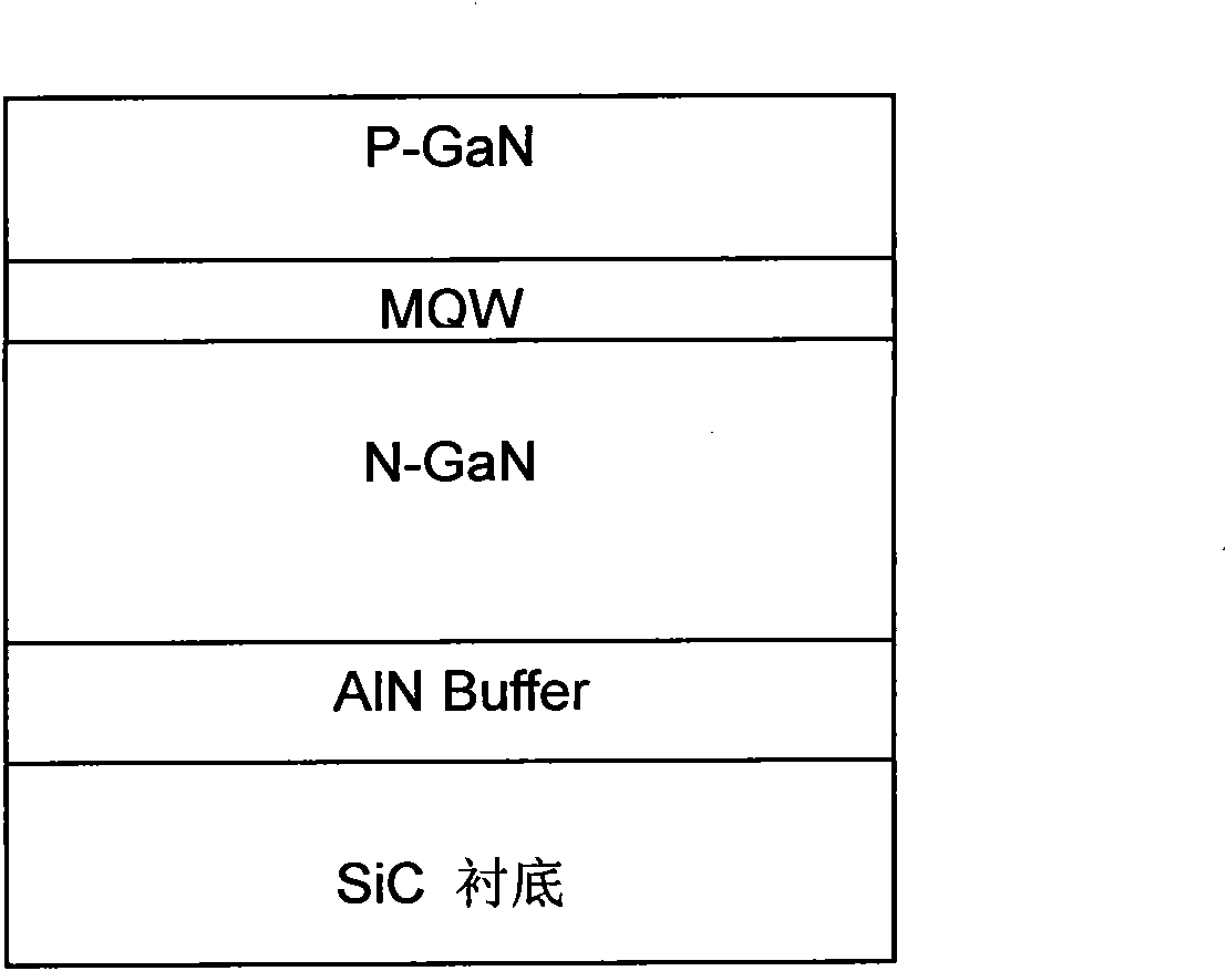
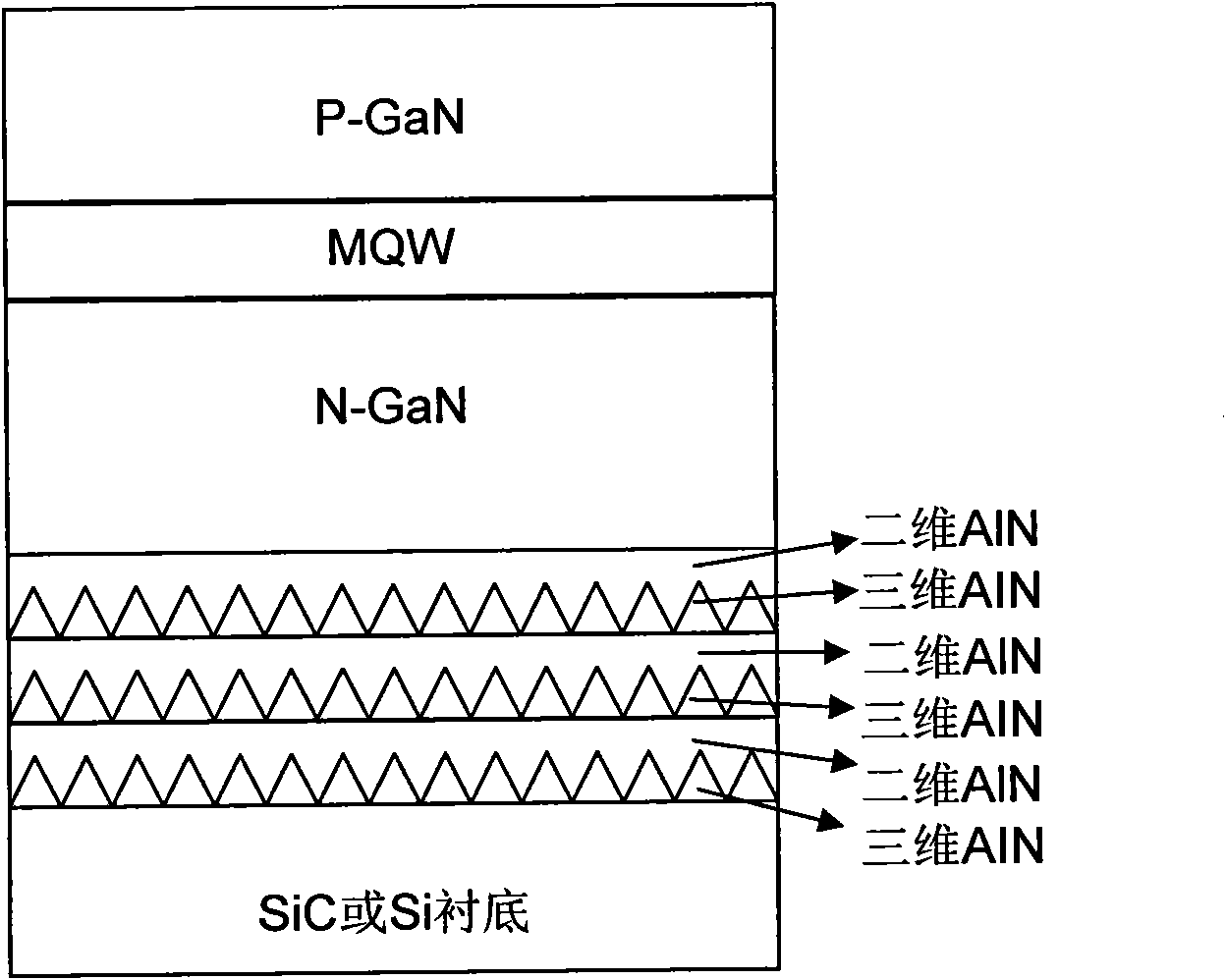
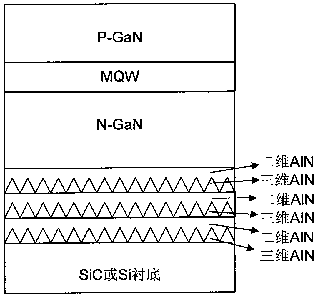
[0023] Such as figure 2 As shown, the present invention also includes SiC or Si substrate, AlN buffer layer, N-type GaN layer, MQW (Multiple Quantum Well) layer and P-type GaN by the structure of the SiC or Si substrate GaN-based crystal grown by resonance in the present invention from bottom to top layer. The AlN buffer layer has 3-5 cycles of three-dimensional and two-dimensional structures. The thickness of three-dimensional AlN is 50nm-100nm, and the thickness of two-dimensional AlN is 30nm-60nm. It is grown by MOCVD (metal organic chemical vapor deposition) method. AlN buffer layer It is obtained by the resonance growth method of three-dimensional and two-dimensional cyclic growth. The specific growth process is:

[0024] (1) First, deposit a layer of high-temperature AlN buffer layer on the SiC or Si substrate at 900°C-1100°C in the MOCVD equipment. The specific process is: first at 900°C-1000°C, NH 3 The three-dimensional growth of AlN (vertical growth rate is great...


PUM


Abstract

The invention provides a structure of SiC or Si substrate GaN-based crystal and a method for growing the same. The structure of the GaN-based crystal, from the bottom to the top, comprises an SiC or Si substrate, an A1N buffer layer, an N-type GaN layer, an MQW and a P-type GaN layer, wherein the A1N buffer layer comprises 3 to 5 three-dimensional and two-dimensional circulations, the thickness of the three-dimensional A1N is 50 to 100 nanometers, and the thickness of the two-dimensional A1N is 30 to 60 nanometers. The method for growing the structure comprises the following steps of: performing the three-dimensional growth of the A1N, wherein the growth thickness is 50 to 100 nanometers; performing two-dimensional growth of the A1N, wherein the growth thickness is 30 to 60 nanometers; circulating the steps for 3 to 5 times; and growing the N-type GaN layer, the MQW layer and the P-type GaN layer. In the method, the A1N is used as the buffer layer, and the three-dimensional and two-dimensional circulation resonant growth of the MOCVD is utilized, so that the dislocation density is effectively reduced, and the dislocation density of the grown film is very low; and because the crystal quality is improved and the stress is released, the thicker full-structure LEDs can be obtained by growth and no crack occurs.

Description

technical field [0001] The invention relates to a method for improving the growth quality of GaN crystals on SiC (silicon carbide) substrates, belonging to the field of optoelectronic technology. Background technique [0002] Group III nitrides represented by GaN (AlN, GaN, InN, AlGaInN) have excellent photoelectric properties, so they are widely used in blue light, green light, ultraviolet light-emitting diodes (LEDs) and high-frequency, high-temperature, high-power electronic devices. application. Due to the lack of lattice-matched substrates, III-nitrides are heteroepitaxy on other materials. Commonly used substrates are sapphire, SiC (silicon carbide), Si (silicon), gallium arsenide, zinc oxide, etc., commonly used The epitaxy methods include metal organic chemical vapor deposition (MOCVD), molecular beam epitaxy (MBE) and hydride vapor phase epitaxy (HVPE). [0003] SiC (silicon carbide) is a wide bandgap semiconductor material, and it has many advantages in applicati...

Claims


Application Information

Patent Timeline
IPC IPC(8): H01L33/12C30B25/16
Inventor 吴德华朱学亮曲爽李毓锋李树强徐现刚
Owner Shandong Huaguang Optoelectronics Co. Ltd.
Learn More