Bulk-silicon processing method for manufacturing microstructure on basis of multiple masking layers

A processing method and technology for a masking layer, which are applied in the manufacture of microstructure devices, microstructure technology, microstructure devices, etc., can solve the problems that the process cannot be carried out smoothly, affecting the second photoresist coating, stacking and degumming, etc. , to avoid stacking and degumming, good compatibility, and flexible operation.

Inactive Publication Date: 2009-12-30
DALIAN UNIV OF TECH
View PDF0 Cites 1 Cited by
  • Summary
  • Abstract
  • Description
  • Claims
  • Application Information

AI Technical Summary

Problems solved by technology

However, it is difficult to realize the fabrication of complex microstructures using traditional silicon technology, because the microstructures produced first in the fabrication process will affect the coating of the second photoresist, which is easy to cause glue stacking and debonding, making subsequent processes impossible. went smoothly

Method used


Image

  • Bulk-silicon processing method for manufacturing microstructure on basis of multiple masking layers

Examples


Embodiment

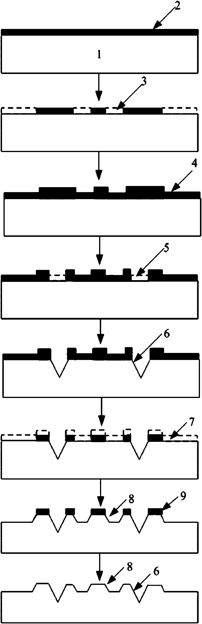
[0016] Example: Silicon dioxide is used as a masking layer to fabricate convex and concave microstructures by wet anisotropic etching technology

[0017] Step 1: Silicon Wafer Oxidation

[0018] Put wafer 1 into H 2 O 2 : H 2 SO 4 =1:3 solution was boiled to smoke for 10min, rinsed with deionized water for 15min, dried to obtain a hydrophobic surface; the treated silicon wafer was placed in a ZKLS-2A double-tube diffusion furnace, heated to 1180°C, and kept for 3.5 hours , a silicon dioxide masking layer 2 with a thickness of 1.5 μm is obtained on the silicon surface.

[0019] Step 2: Photolithography

[0020] Coat BP212 photoresist evenly on the silicon wafer obtained in step 1. The pre-spin coating time is 5s, the spin coating time is 30s, the pre-spin coating speed is 500rpm, and the spin coating speed is 3000rpm; the pre-bake BP212 photoresist is at 85℃ In the oven for 20min; after cooling, it was exposed on a BGJ-3 type lithography machine, and the light intensity o...


PUM

PropertyMeasurementUnit
thicknessaaaaaaaaaa

Abstract

A complex microstructure manufactured by the conventional silicon process is susceptible to glue heap and stripping problems during secondary spin coating and photoetching, so that the manufacturing of the microstructure on a silicon substrate cannot be performed. The invention discloses a bulk-silicon processing method for manufacturing a microstructure on basis of multiple masking layers, belongs to the field of silicon process manufacturing, and is used for realizing the manufacturing of a complex microstructure on a silicon chip. The method uses masking layer growing and nesting technology to transfer patterns on a plurality of masks onto the silicon chip layer by layer and complete all photoetching steps related to the whole process, thereby solving the glue heap and stripping problems caused by the existence of the silicon microstructure and realizing the manufacturing of a micro complex structure on the silicon chip. The method has the advantages of solving the problem of difficult manufacturing of the micro complex structure in the conventional silicon process, along with excellent compatibility with the conventional silicon process as well as flexible operation and simplicity.

Description

technical field [0001] The invention belongs to the technical field of silicon process manufacturing, and relates to a new bulk silicon processing method for manufacturing microstructures based on multi-layer masking layers, which is used to realize the manufacture of complex microstructures on silicon wafers. Background technique [0002] Silicon process technology is the basis of electronic manufacturing technology. The field of micro / nano electromechanical (M / NEMS) draws on related technologies of electronic manufacturing, especially silicon process technology, and has made breakthroughs in many aspects. However, with the continuous improvement of device functions, the structures on the device have also become diversified, so it is necessary to continuously innovate on the basis of traditional silicon technology to meet the production requirements of new silicon structures. [0003] Except for some simple boss and groove structures, many complex structures cannot be proce...

Claims


Application Information

Patent Timeline
Patent Type & Authority Applications(China)
IPC IPC(8): B81C1/00
Inventor 罗怡张宗波王晓东张彦国郑英松
Owner DALIAN UNIV OF TECH
Why Eureka
Try Eureka