Ultra-large-scale staring infrared detector splicing substrate and its preparation method

An infrared detector and ultra-large-scale technology, applied in the field of infrared detectors, can solve problems such as the difficulty of preparing infrared detector arrays, achieve the effects of improving fluidity and flatness, and improving splicing accuracy

Active Publication Date: 2020-12-18
11TH RES INST OF CHINA ELECTRONICS TECH GROUP CORP
View PDF6 Cites 0 Cited by
  • Summary
  • Abstract
  • Description
  • Claims
  • Application Information

AI Technical Summary

Problems solved by technology

[0003] Embodiments of the present invention provide a super-large-scale staring infrared detector splicing substrate and a preparation method thereof, to solve the problem that a super-large-scale infrared detector array is difficult to manufacture in the prior art

Method used


Image

  • Ultra-large-scale staring infrared detector splicing substrate and its preparation method
  • Ultra-large-scale staring infrared detector splicing substrate and its preparation method
  • Ultra-large-scale staring infrared detector splicing substrate and its preparation method

Examples


Embodiment Construction

[0035] Exemplary embodiments of the present disclosure will be described in more detail below with reference to the accompanying drawings. While exemplary embodiments of the present disclosure are shown in the drawings, it should be understood that the present disclosure may be embodied in various forms and should not be limited by the embodiments set forth herein. Rather, these embodiments are provided so that the present disclosure will be more thoroughly understood, and will fully convey the scope of the present disclosure to those skilled in the art.

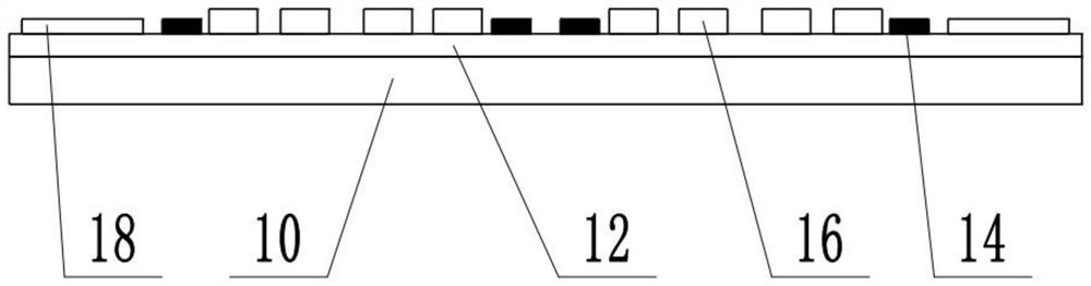
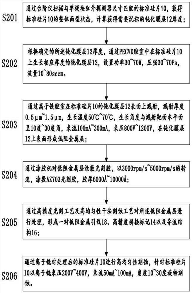
[0036] The embodiment of the present invention provides a super large-scale staring infrared detector splicing substrate, such as figure 1 As shown, it includes: a standard silicon wafer 10, a passivation film layer 12 and a low-resistance metal layer, wherein the low-resistance metal layer specifically includes: a high-precision splicing mark 14 formed by etching the low-resistance metal layer, and a diversion structure 16 ...


PUM


Abstract

The invention discloses a super-large scale staring infrared detector spliced base plate. The super-large scale staring infrared detector spliced base plate comprises a standard silicon wafer, a passive film layer and low resistance metal layer, wherein the low resistance metal layer specifically comprises a high-precision splicing mark formed by etching the low resistance metal layer, a current guiding structure and a pair of low resistance metal wires; the passive film layer is arranged on an upper surface of the standard silicon wafer, the pair of low resistance metal wires is arranged at two sides of the upper surface of the passive film layer, the high-precision splicing mark is arranged on the upper surface of the passive film layer between the pair of low resistance metal wires, andthe current guiding structure is arranged between the pair of low resistance metal wires and located on the upper surface of the passive film layer where the high-precision splicing mark is not existent. According to the super-large scale staring infrared detector spliced base plate provided by the invention, the highly smooth passive film layer, the high-precision splicing mark, the current guiding structure and the low-resistance value metal wires are manufactured, thus, splicing precision of a staring infrared detector is improved, low-loss output of signals is facilitated, and a problem that a super-large scale infrared detector array in the prior art is difficult to prepare is solved

Description

technical field [0001] The invention relates to the field of infrared detectors, in particular to an ultra-large-scale staring-type infrared detector splicing substrate and a preparation method thereof. Background technique [0002] Infrared detector components, especially mercury cadmium telluride infrared focal plane detector components, promote the development of infrared technology applications, greatly improve the performance of infrared weapons and equipment, and become an important part of advanced optoelectronic weapon systems. In the application of space missile early warning satellites, space-based and ground-based early warning systems, satellite remote sensing, space astronomical detection and other aerospace model systems, the need for ultra-large-scale infrared detector arrays is becoming more and more urgent. The fabrication of ultra-large-scale staring infrared detector arrays requires high-precision splicing of multiple single-die modules. Different from th...

Claims


Application Information

Patent Timeline
Patent Type & Authority Patents(China)
IPC IPC(8): H01L31/09H01L31/0216H01L31/18
CPCY02P70/50
Inventor 张敏亢喆韦书领刘明杨刚
Owner 11TH RES INST OF CHINA ELECTRONICS TECH GROUP CORP
Why Eureka
Try Eureka