Method for preparing hollowed-out polyimide evaporation shadow mask

A technology of polyimide and evaporation mask, which is applied in the field of preparing hollowed-out polyimide evaporation mask stencil, which can solve the problems of large thickness of metal substrate, high price, difficulty in ensuring accurate size of stencil pattern, etc. , to achieve the effect of neat edges, low process cost and precise graphic size

Active Publication Date: 2009-10-28
INST OF MICROELECTRONICS CHINESE ACAD OF SCI
View PDF0 Cites 9 Cited by
  • Summary
  • Abstract
  • Description
  • Claims
  • Application Information

AI Technical Summary

Problems solved by technology

At present, the most widely used metal stencil is the metal stencil. The metal substrate used when making the mask stencil with metal materials is relatively thick, about tens or even hundreds of microns. Large lateral corrosion brings insurmountable obstacles to the production of high-precision and high-resolution metal stencils. It is difficult to ensure precise dimensions and neat edges for stencil graphics
In addition, metal stencil production takes a long time and is expensive, which is not suitable for research and production

Method used


Image

  • Method for preparing hollowed-out polyimide evaporation shadow mask
  • Method for preparing hollowed-out polyimide evaporation shadow mask
  • Method for preparing hollowed-out polyimide evaporation shadow mask

Examples


Embodiment Construction

[0024] In order to make the object, technical solution and advantages of the present invention clearer, the present invention will be described in further detail below in conjunction with specific embodiments and with reference to the accompanying drawings.

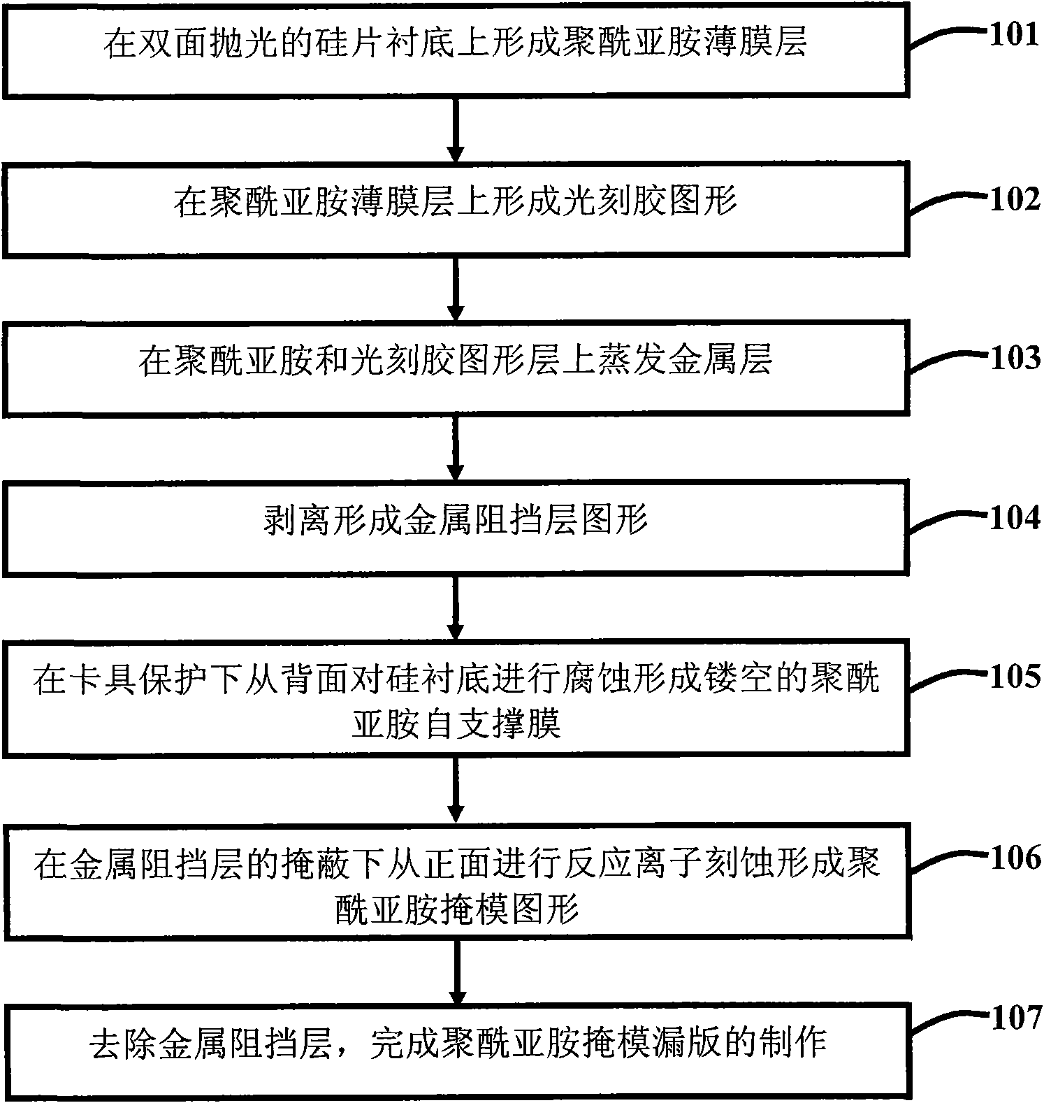
[0025] Such as figure 1 as shown, figure 1 It is a flow chart of a method for preparing a hollowed-out polyimide evaporation mask stencil provided by the present invention, and the method includes the following steps:

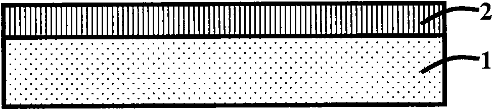
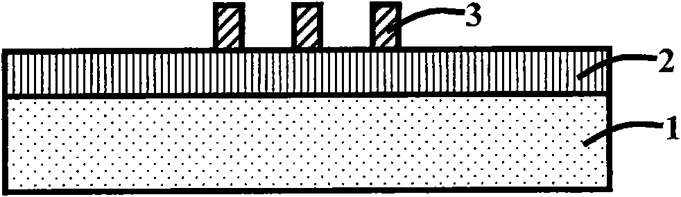
[0026] Step 101: forming a polyimide film layer 2 on a double-sided polished silicon wafer substrate 1;

[0027] In this step, a double-throw silicon wafer with high resistivity and (100) crystal orientation is used as the substrate. The formation of polyimide film layers is obtained by low-cost solution processing methods such as spin-coating polyimide precursors. The thickness of the film is adjusted by rotation speed and solution concentration. After spin-coating, it needs to be baked in two steps: ...


PUM


Abstract

The invention discloses a method for preparing an evaporation shadow mask for manufacturing semiconductor devices, which comprises the process steps: 1, forming a polyimide film layer on a silicon chip substrate with double-sided polishing; 2, forming a photoresist pattern on the polyimide film layer; 3, evaporating a metal layer on a polyimide layer and a photoresist pattern layer; 4, peeling to form a metal barrier layer; 5, corroding a silicon substrate from the back side under the protection of a fixture to form a hollowed-out polyimide self-supporting film; 6, performing reactive ion etching from the right side under the masking of the metal barrier layer to form a polyimide mask pattern; and 7, removing the metal barrier layer to finish the production of a polyimide shadow mask. The method for producing the shadow mask by utilizing a polyimide material has small process difficulty, high precision of graphic dimensions and low manufacturing cost, and is suitable for large-area graphization process of the field of the preparation of organic semiconductor devices.

Description

technical field [0001] The invention belongs to the field of microfabrication in semiconductor science, and relates to a preparation technology of an evaporation mask for semiconductor device preparation, in particular to a method for preparing a hollow polyimide evaporation mask stencil. Background technique [0002] It is inevitable to pattern each functional material layer in the fabrication of semiconductor devices. In traditional silicon technology, photolithography is often used for pattern definition. However, in the preparation of organic semiconductor devices, due to the sensitivity of organic materials to photoresist and developer, the method of lithography to define patterns is greatly limited. Therefore, patterning using a shadow mask is widely used. The metal stencil is the most widely used at present. The thickness of the metal substrate used when making the mask stencil with metal materials is relatively large, about tens or even hundreds of microns. Large ...

Claims


Application Information

Patent Timeline
Patent Type & Authority Applications(China)
IPC IPC(8): G03F7/12G03F7/00
Inventor 甄丽娟商立伟刘明刘兴华涂德钰刘舸
Owner INST OF MICROELECTRONICS CHINESE ACAD OF SCI
Why Eureka
Try Eureka