Process for producing superconducting oxide material
A manufacturing method and oxide technology, applied in chemical instruments and methods, cable/conductor manufacturing, copper compounds, etc., can solve problems such as difficulty in controlling orientation, decrease in uniformity, etc., and achieve improved superconducting properties and high manufacturing efficiency. , suitable for mass production
- Summary
- Abstract
- Description
- Claims
- Application Information
AI Technical Summary
Problems solved by technology
Method used
Image
Examples
Embodiment 1
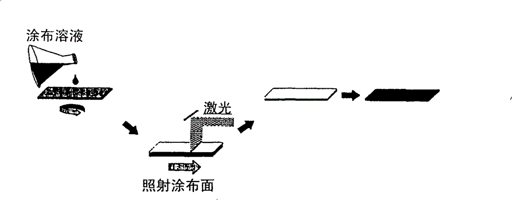
[0117] The coating solution Y1 was spin-coated on the substrate KCl at 4000 rpm for 10 seconds, dried in a constant temperature bath at 130°C in order to remove the solvent, and then the coated surface was irradiated with laser light H1 at room temperature. At this time, the intensity of the laser is set to 16.4mJ / cm 2 The laser scans in one direction, and irradiates with pulse numbers of 10,000, 20,000, 30,000, and 40,000 on one side.
[0118] Other irradiation conditions are as follows.
[0119] room temperature, atmosphere
[0120] Frequency: 100Hz
[0121] Overlap rate: 99%
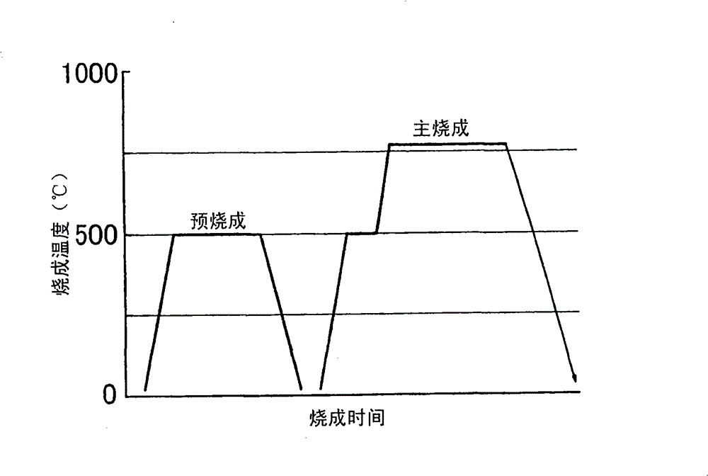
[0122] Next, the laser-irradiated sample was inserted into a muffle furnace previously kept at 500° C., kept at this temperature for 30 minutes, and then taken out. Then, main firing was performed in a quartz tubular furnace under the following conditions.
[0123] First, in the mixed gas flow of argon and oxygen with the oxygen partial pressure adjusted to 100ppm, the temperature was raised to 7...
Embodiment 2
[0129] For comparison, except that laser irradiation is not carried out, other YBCO films with a film thickness of about 100nm made in the same manner as in Example 1, the Jc obtained by the induction method is within the detection limit (0.1MA / cm 2 )the following.
Embodiment 3
[0131] In addition to making the laser intensity 11mJ / cm 2 , the number of pulses is 500, and the amount of total energy is 5.5J / cm 2 In addition, other YBCO films with a film thickness of about 100 nm produced in the same manner as in Example 1 had a Jc of 1.1 MA / cm obtained by the induction method. 2 .
PUM
| Property | Measurement | Unit |
|---|---|---|
| thickness | aaaaa | aaaaa |
| strength | aaaaa | aaaaa |
| strength | aaaaa | aaaaa |
Abstract
Description
Claims
Application Information
 - R&D
- Intellectual Property
- Life Sciences
- Materials
- Tech Scout
- Unparalleled Data Quality
- Higher Quality Content
- 60% Fewer Hallucinations
Browse by: Latest US Patents, China's latest patents, Technical Efficacy Thesaurus, Application Domain, Technology Topic, Popular Technical Reports.
© 2025 PatSnap. All rights reserved.Legal|Privacy policy|Modern Slavery Act Transparency Statement|Sitemap|About US| Contact US: help@patsnap.com


