Manufacturing method of light emitting diode
A technology for light-emitting diodes and manufacturing methods, which is applied to lasers, phonon exciters, laser components, etc., can solve the problems of non-conformity with commercial applications of light-emitting diodes, increase costs, and cumbersome manufacturing processes, so as to improve internal quantum efficiency and reduce The probability of total reflection and the effect of reducing threading dislocations
- Summary
- Abstract
- Description
- Claims
- Application Information
AI Technical Summary
Problems solved by technology
Method used
Image
Examples
no. 1 example
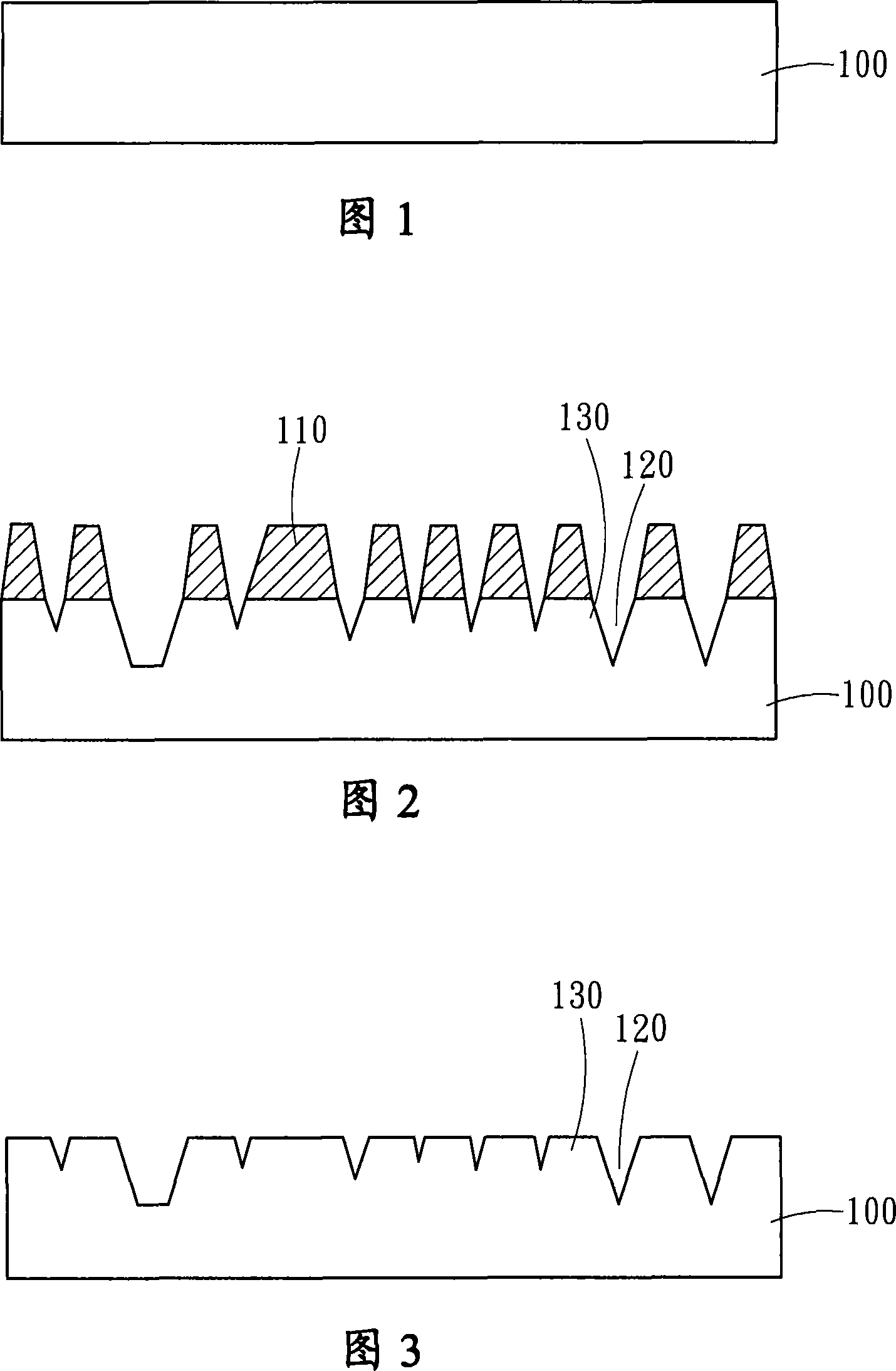
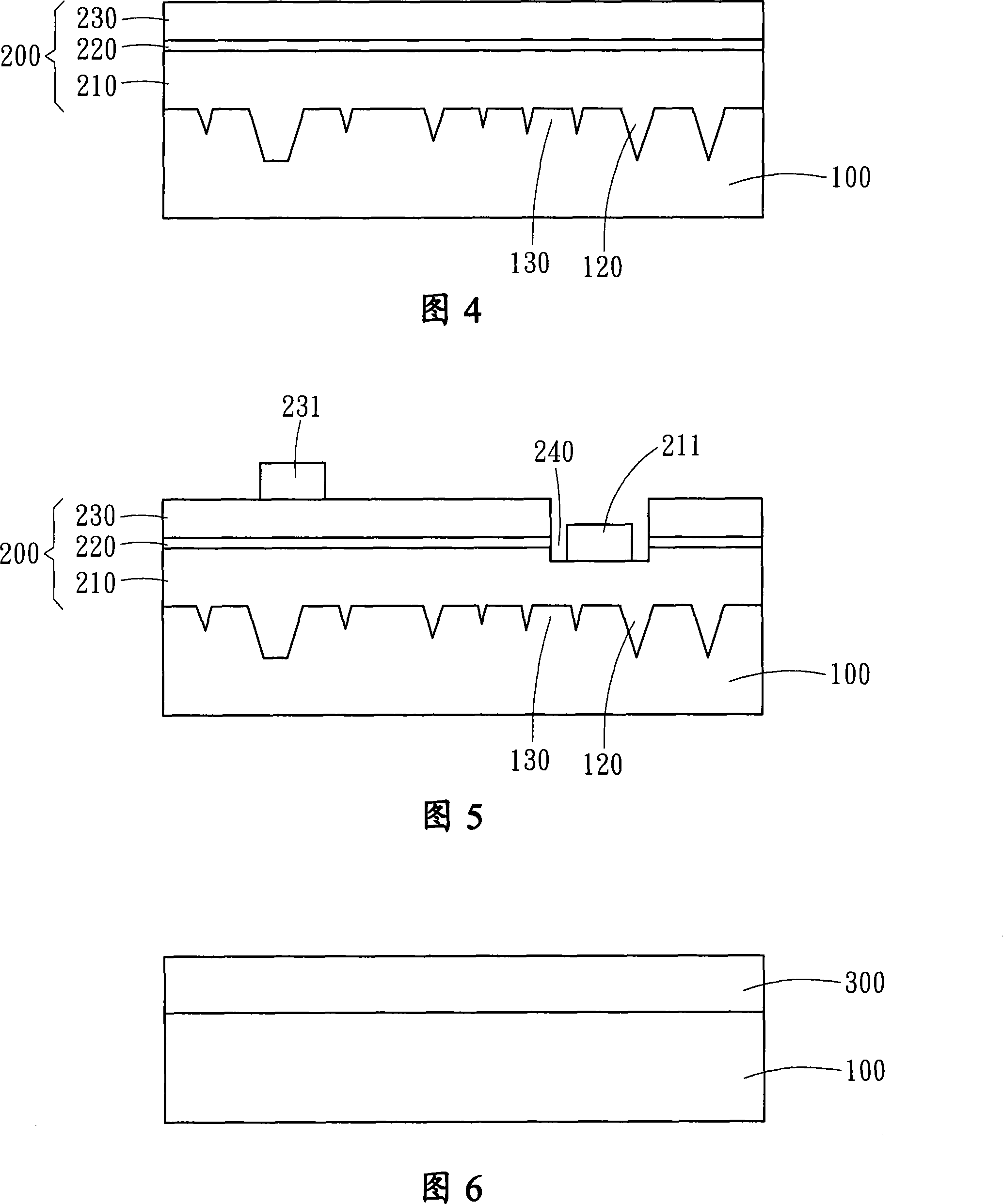
[0028] Please refer to FIG. 1 to FIG. 5 , which are schematic diagrams of the first embodiment of the present invention. The manufacturing method of the present invention at least includes: first providing a substrate 100, which is one of sapphire, silicon carbide, silicon, gallium arsenide, aluminum nitride and gallium nitride (as shown in FIG. 1 ).
[0029]Then the substrate 100 is placed in a first solution for reaction, so that a high-density nanoscale chemical reaction layer 110 is naturally formed on the surface of the substrate 100 . The substrate 100 is placed in the first solution for 1 second to 200 minutes, and then the chemical reaction layer 110 is used as a mask to selectively etch the substrate 100. Dry etching, wet etching and other methods can be used. Selective etching, one of the mixed methods, forms a plurality of recesses 120 and protrusions 130 with the chemical reaction layer 110 on the surface of the substrate 100 without the chemical reaction layer 110...
no. 2 example
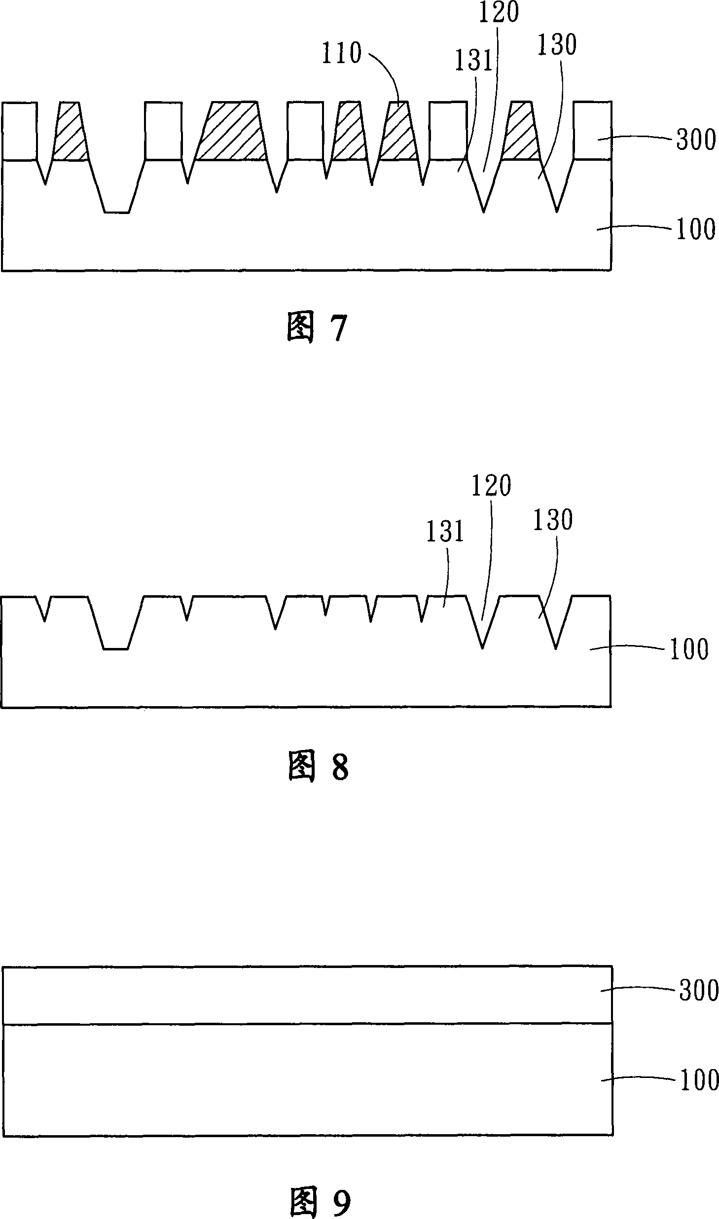
[0041] Please refer to the schematic diagrams of the second embodiment of the present invention shown in FIG. 6 to FIG. 8 . The manufacturing method of this embodiment is based on the first embodiment, but the substrate 100 is subjected to a pretreatment process before being placed in the first solution. The pretreatment process grows a thickness of 1 A passivation layer 300 to 10 μm is formed on the surface of the substrate 100 (as shown in FIG. 6 ). The material of the passivation layer 300 can be one of silicon, silicon nitride, silicon oxide, aluminum oxide, metal, photoresist, benzocyclobutene, polyimide single-layer structure, multi-layer structure and combinations thereof.
[0042] Then place the substrate 100 in the first solution to react, so that a high-density nanoscale chemical reaction layer 110 is naturally formed in the passivation layer 300 on the surface of the substrate 100, and then the passivation layer 300 and the chemical reaction layer 110 is used as ...
no. 3 example
[0045] Please refer to FIG. 9 to FIG. 13 , which are schematic diagrams of the third embodiment of the present invention. The manufacturing method of this embodiment is based on the second embodiment, and the pretreatment process is the same as growing the passivation layer 300 on the surface of the substrate 100 (as shown in FIG. 9 ). Then, the passivation layer 300 is further periodically patterned through a yellow light lithography process to expose a part of the surface of the substrate 100, wherein the periodic pattern of the passivation layer 300 is a periodic pattern of a circle, a polygon and a combination thereof. The width of the pattern is 0.1 micron to 15 microns, and the pitch is 0.1 micron to 15 microns (as shown in Figure 10).
[0046] Then place the substrate 100 in the first solution to react, so that the exposed surface of the substrate 100 naturally forms a high-density nanoscale chemical reaction layer 110 (as shown in FIG. 11 ). Then, using the passivatio...
PUM
 Abstract
Description
Claims
Application Information
 - R&D
- Intellectual Property
- Life Sciences
- Materials
- Tech Scout
- Unparalleled Data Quality
- Higher Quality Content
- 60% Fewer Hallucinations
Browse by: Latest US Patents, China's latest patents, Technical Efficacy Thesaurus, Application Domain, Technology Topic, Popular Technical Reports.
© 2025 PatSnap. All rights reserved.Legal|Privacy policy|Modern Slavery Act Transparency Statement|Sitemap|About US| Contact US: help@patsnap.com


