Method for constructing anti-reflection microstructure using single layer nanometer particle as etching blocking layer
A technology for etching barrier layers and nanoparticles, which is applied in the field of surface patterned microstructure construction, can solve problems such as complex processes, and achieve the effects of good repeatability, simple method and strong applicability
- Summary
- Abstract
- Description
- Claims
- Application Information
AI Technical Summary
Problems solved by technology
Method used
Image
Examples
Embodiment 1
[0067] The aqueous solution of PS spheres can use 2% sodium lauryl sulfate solution to form a monolayer ordered structure on the water surface, and this monolayer structure can be transferred to a single crystal silicon [n type, (100)] substrate. (Kluwer Academic Publishers, Dordeecht. 2003, p. 163-172).
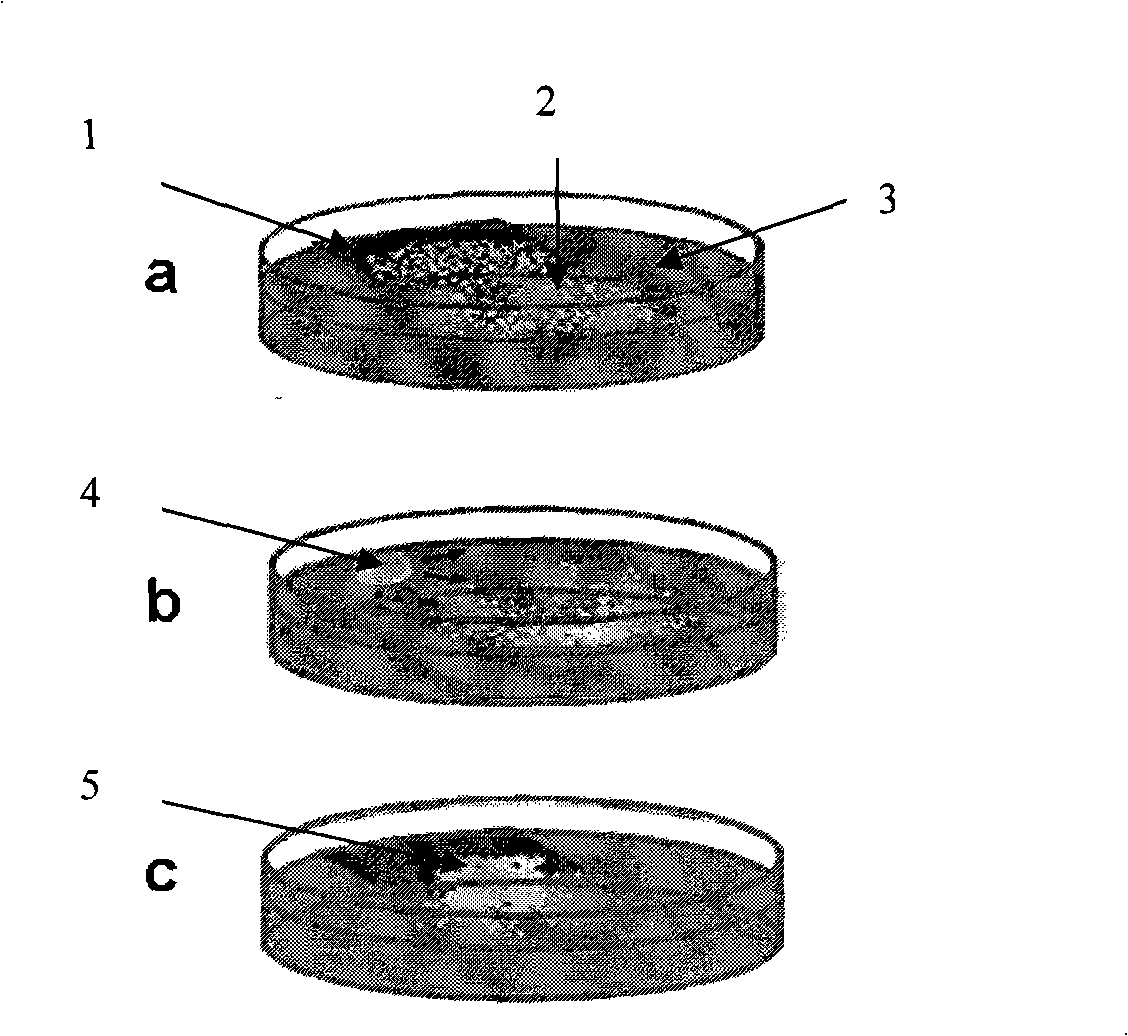
[0068] Technical parameters of self-assembled monolayer spheres: PS solution with a mass fraction of 10% was purchased from Microparticles GmbH (Germany), mixed with ethanol in an equal volume, and supercharged for 15 minutes before use. Add 150 mL of high-purity water (treated by a French MILLI~Q ultrapure water instrument, with a resistivity of 18.2 MΩcm) into a glass petri dish with a diameter of 15 cm, and drop 5 μL of the prepared solution onto a silicon wafer with a clean surface and a hydrophilic treatment. At this time, the PS microspheres disperse on the water surface to form a disordered structure, such as figure 1 a, After waiting for 50 minutes, add 5 μL of 2% ...
Embodiment 2
[0070] Assemble the silylating agent of one deck amino on silicon chip, utilize amino group to adsorb silver nanoparticle, so just obtained a monolayer film (S.Wang, X. Z. Yu, H. T. Fan, Appl. Phys. Lett. 2007, 91, 061105(1-3)).
[0071] Put the treated clean and dry monocrystalline silicon (or quartz, glass) substrate into a vacuum desiccator that has been dripped with an aminosilane reagent (trimethoxypropylaminosilane) in advance, and keep the vacuum degree of the vacuum desiccator at 0.012Pa After standing for 40 minutes, take it out and clean it sequentially with toluene, chloroform, and ethanol solvents, 3 minutes each time, and then use deionized water to clean it twice, 3 minutes each time, and then dry it with nitrogen, and then the modified aminosilane reagent monomolecular film The silicon wafer was soaked in the solution of metallic silver nanoparticles prepared by literature method (S.D.Stahaye, K.R.Patil, S.R.Padalkar, Materials research bulletin, 2001, 36, 1149-...
Embodiment 3
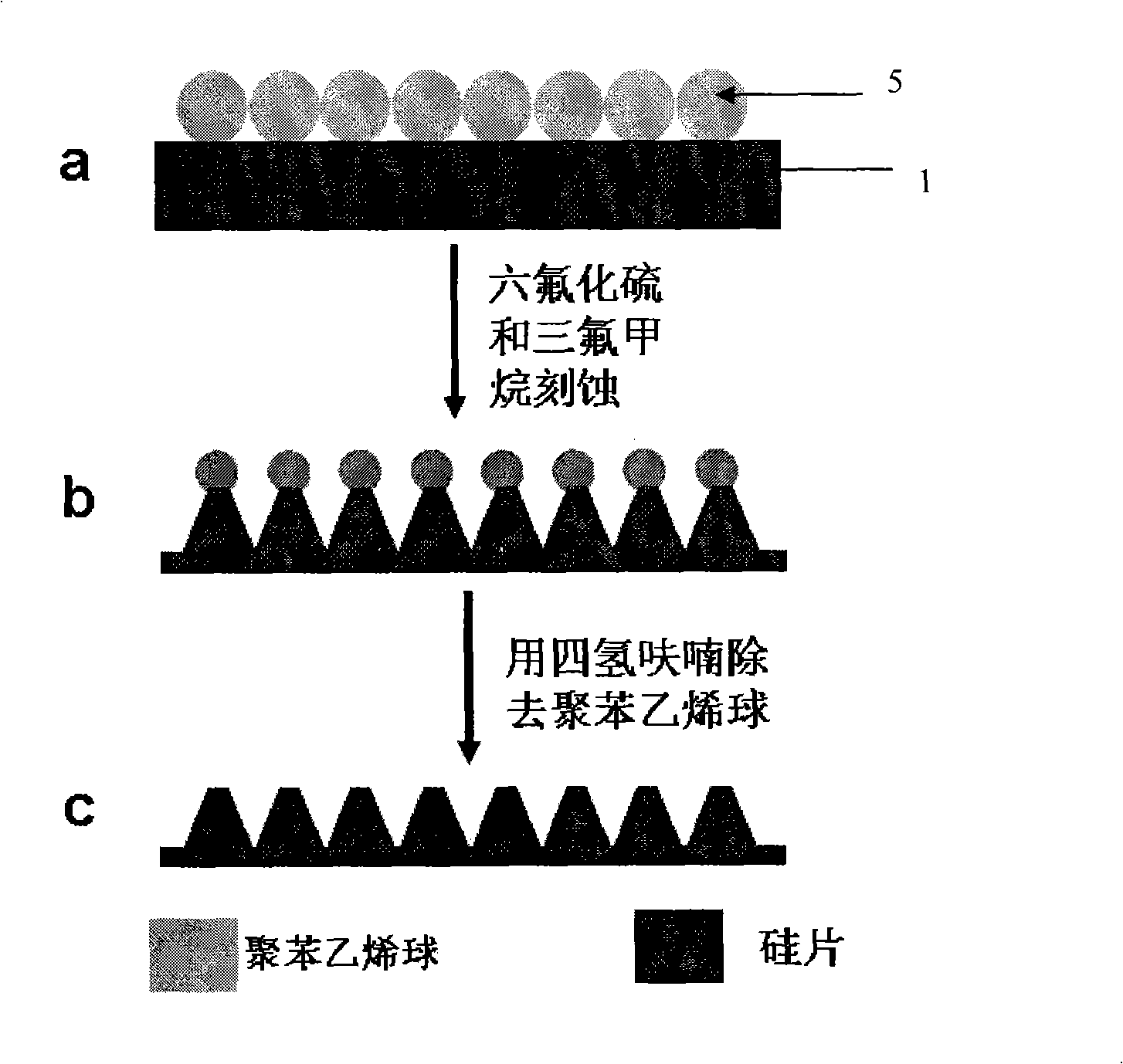
[0073] Take 600mL of high-purity water (treated by a French MILLI~Q ultrapure water instrument, with a resistivity of 18.2MΩcm) into a glass container with a diameter of 12cm, and place a ring of polytetrafluoroethylene with a diameter of 10cm on the water surface. The water surface in the ring is magnetically stirred, and its rotation speed is 120rpm, and the water surface forms a meniscus under the stirring of the magnetic force. At this time, in the meniscus, 5% PS ball aqueous solution (Feng Pan, Junying Zhang, Chao Cai) is added dropwise. , and Tianmin Wang, Langmuir, 2006, 22, 7101-71014). Under the action of centrifugal force, the PS spheres on the water surface self-organize to form an ordered monolayer PS sphere structure, and the microstructure of the ordered monolayer PS spheres is transferred to the substrate (such as silicon, glass, polymer, etc.) by vertical pulling method. and other cleaned and hydrophilic treated substrates). Then the obtained sample was etche...
PUM
 Abstract
Description
Claims
Application Information
 - R&D
- Intellectual Property
- Life Sciences
- Materials
- Tech Scout
- Unparalleled Data Quality
- Higher Quality Content
- 60% Fewer Hallucinations
Browse by: Latest US Patents, China's latest patents, Technical Efficacy Thesaurus, Application Domain, Technology Topic, Popular Technical Reports.
© 2025 PatSnap. All rights reserved.Legal|Privacy policy|Modern Slavery Act Transparency Statement|Sitemap|About US| Contact US: help@patsnap.com


