


Quick Research
Generate reliable direction feasibility study reports for your R&D in just a few steps.

Technical Q&A
Discover and master advanced knowledge NOW. Basics, ideas, possibilities, all at once.

Find Solutions
As an expert in R&D theories, this can generate solutions to your technical problems instantly.

Evaluate Feasibility
Analyze your overall solution with one click, know your potential R&D risks in advance.

Monitor Landscape
Get weekly tech updates, stay abreast of the latest tech innovations and key insights.
Method for manufacturing DRAM capacitor structure and formed structure
A capacitor structure and capacitor technology, which are applied in the manufacture of capacitors, electric solid-state devices, semiconductor/solid-state devices, etc., can solve the problems of complex manufacturing process and structure, difficult manufacturing, large capacitance value, etc., and achieve high device yield and improved process. The effect of integration
- Summary
- Abstract
- Description
- Claims
- Application Information
AI Technical Summary
Problems solved by technology
Method used
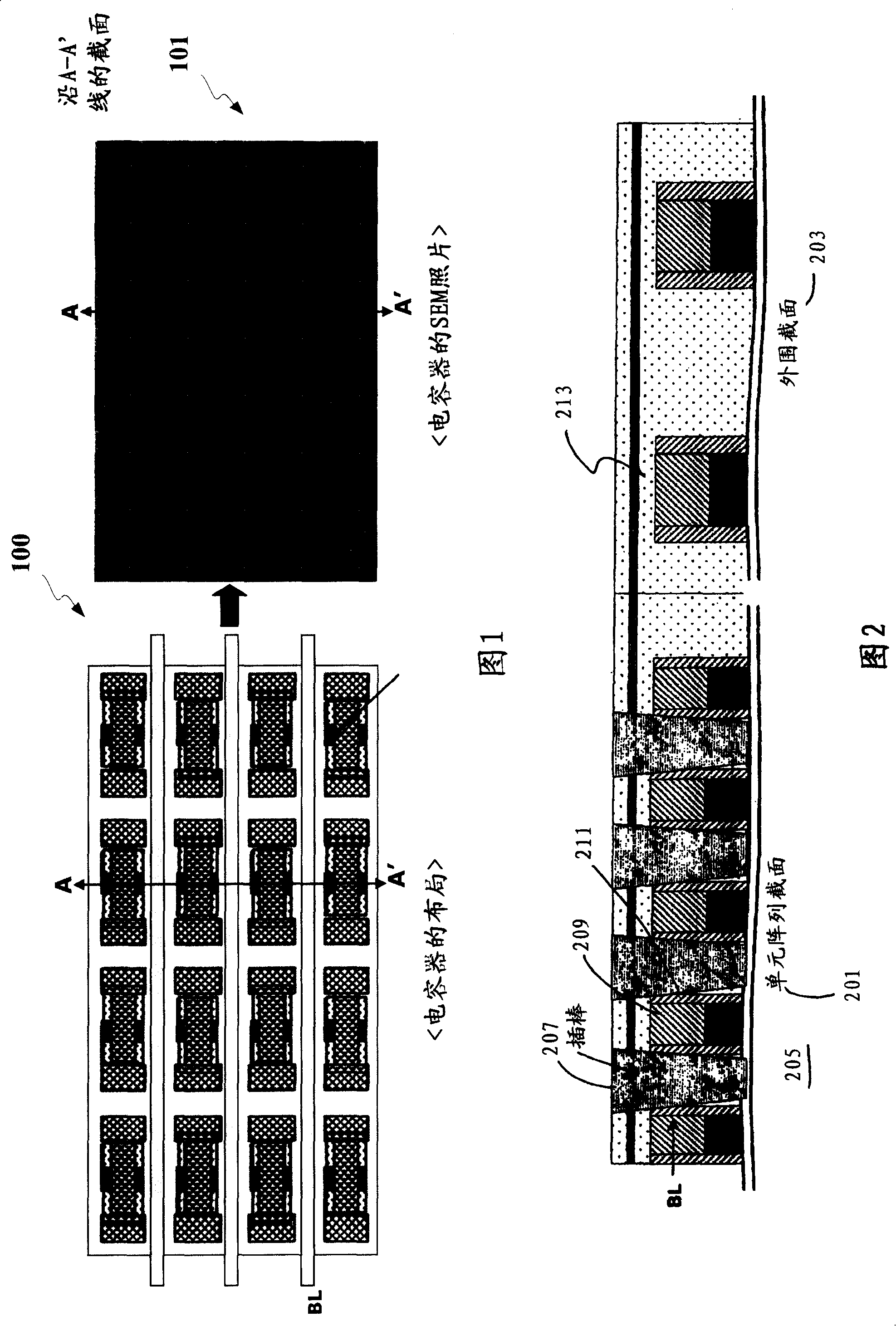
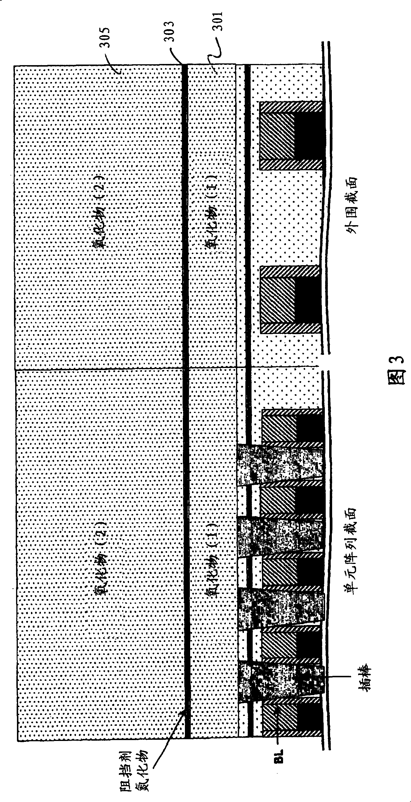
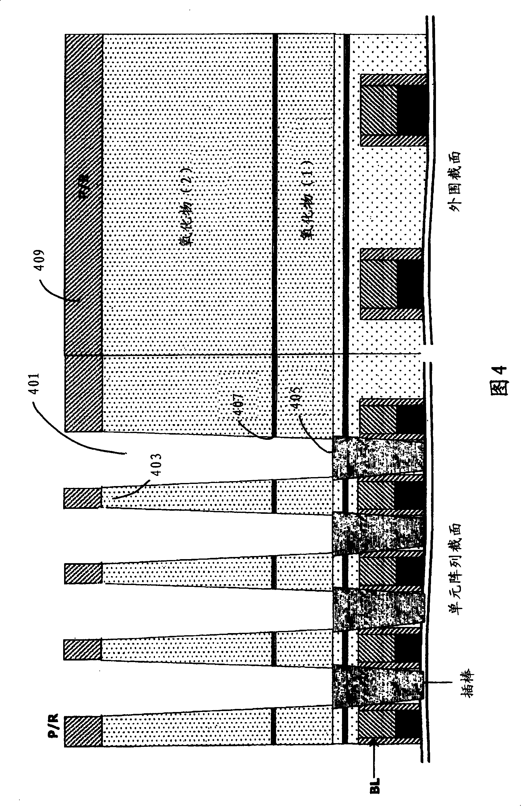
Image

Examples
Embodiment Construction
[0012] According to the present invention, there is provided a processing technique for integrated circuits for semiconductor device fabrication. In particular, the present invention provides methods and structures for fabricating capacitors for dynamic random access memory, commonly referred to as DRAM. It should be recognized, however, that the scope of the invention is much broader.
[0013] According to an embodiment of the present invention, a method of forming a capacitor structure for a dynamic random access memory is outlined as follows:
[0014] 1. Provide semiconductor substrate;
[0015] 2. Form a device layer (such as a MOS transistor) covering the semiconductor substrate;
[0016] 3. forming a first interlayer dielectric covering the device layer, preferably, the first interlayer dielectric is planarized;
[0017] 4. Forming a through-hole structure (such as a plug) in the first interlayer dielectric layer;
[0018] 5. forming a first oxide layer overlying the...
PUM
 Abstract
Description
Claims
Application Information
 - R&D Engineer
- R&D Manager
- IP Professional
- Industry Leading Data Capabilities
- Powerful AI technology
- Patent DNA Extraction
Browse by: Latest US Patents, China's latest patents, Technical Efficacy Thesaurus, Application Domain, Technology Topic, Popular Technical Reports.
© 2024 PatSnap. All rights reserved.Legal|Privacy policy|Modern Slavery Act Transparency Statement|Sitemap|About US| Contact US: help@patsnap.com