
Silicon based compliant substrate material for zinc oxide epitaxial film growth

A technology of epitaxial thin film and substrate materials, applied in the direction of electrical components, electrical solid devices, circuits, etc., to achieve the effects of simple structure, reduced residual stress, and improved crystal quality

Inactive Publication Date: 2009-09-30
INST OF SEMICONDUCTORS - CHINESE ACAD OF SCI
View PDF3 Cites 0 Cited by
  • Summary
  • Abstract
  • Description
  • Claims
  • Application Information

AI Technical Summary

Problems solved by technology

There are two reasons for the analysis. On the one hand, the development of the preparation and growth technology of ZnO epitaxial thin film is still in development. On the other hand, there is no more suitable covariable layer that meets the basic conditions of the ideal covariable intermediate layer.

Method used


Image

  • Silicon based compliant substrate material for zinc oxide epitaxial film growth
  • Silicon based compliant substrate material for zinc oxide epitaxial film growth
  • Silicon based compliant substrate material for zinc oxide epitaxial film growth

Examples


Embodiment 1

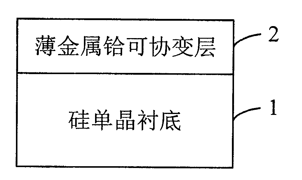
[0053] Using the ion beam epitaxy method, a 27nm-thick metal hafnium (α-Hf) compliant layer (sample P1) 2 was prepared and grown on a Si(111) substrate 1 to form a silicon-based compliant substrate.

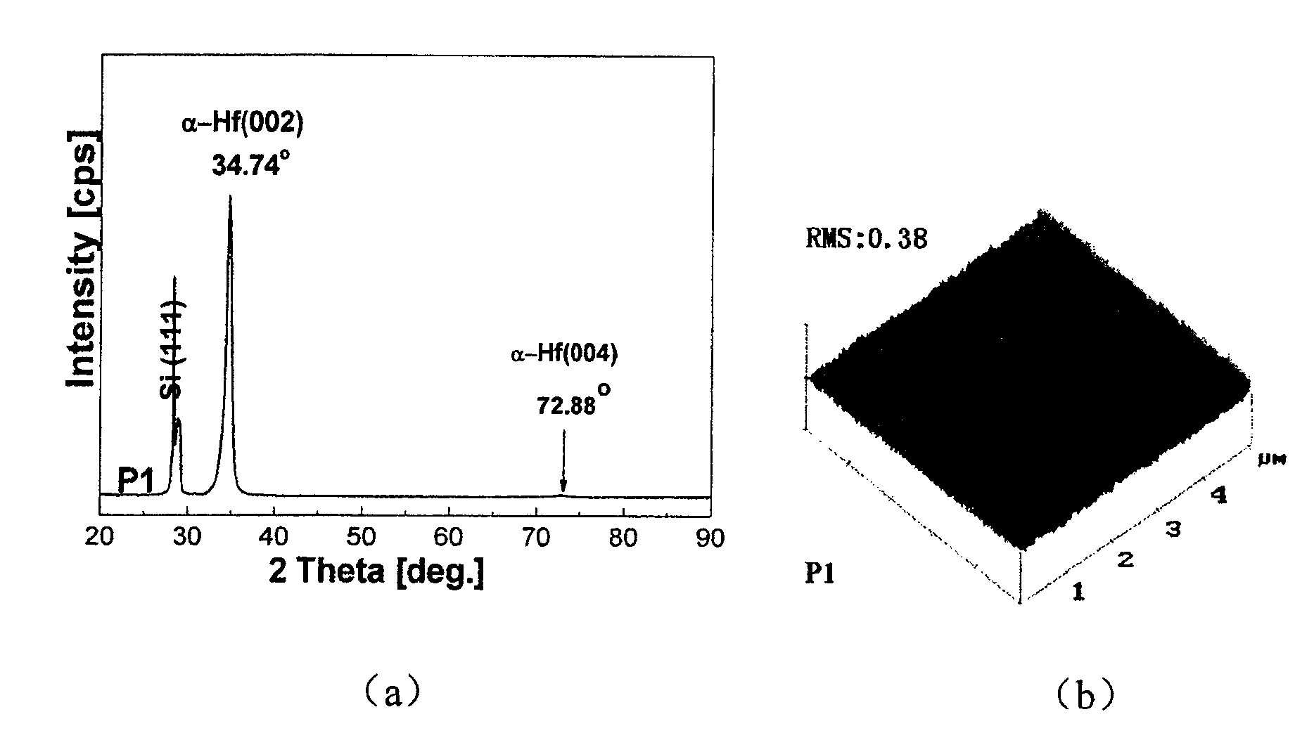
[0054] Depend on figure 2 In (a) X-ray diffraction (XRD) and (b) atomic force surface morphology (AFM) test analysis results, it can be seen that the prepared thin metal hafnium (α-Hf) covariable layer 2 has hexagonal α-Hf ( 100) single preferred orientation, the surface is relatively smooth and flat, and the root mean square roughness value of the surface by AFM is 0.38nm.

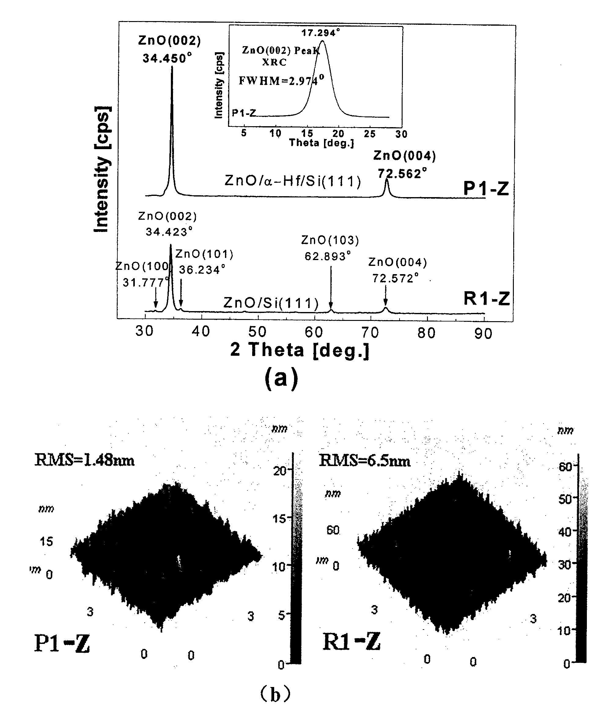
[0055] Zinc oxide epitaxial films 3 with the same thickness were prepared on the silicon-based variable substrate and the common Si(111) substrate by using the same magnetron sputtering process.

[0056] Depend on image 3 In (a) X-ray diffraction (XRD) test and analysis results, it can be seen that the zinc oxide epitaxial thin film sample R1-Z directly grown on the ordinary Si(111) substrate has poor cr...

Embodiment 2

[0059] A 27nm-thick metal hafnium compliant layer (sample P2) 2 was grown on a Si(100) substrate 1 by ion beam epitaxy, forming a silicon-based compliant substrate.

[0060] Depend on Figure 4 In (a) X-ray diffraction (XRD) and (b) atomic force surface morphology (AFM) test analysis results, it can be seen that the prepared thin metal hafnium covariable layer 2 has a single preferred orientation of hexagonal α-Hf(002) , the surface is relatively smooth and flat, and the root mean square roughness of the surface of the P2 sample AFM is 0.89nm.

[0061] Zinc oxide epitaxial films 3 with the same thickness were prepared on the silicon-based variable substrate and the common Si(100) substrate by using the same magnetron sputtering process.

[0062] Depend on Figure 5 In (a) X-ray diffraction (XRD) test and analysis results, it can be seen that the crystal quality of the zinc oxide epitaxial film sample T2-Z grown directly on the ordinary Si(100) substrate is obviously inferior...


PUM

PropertyMeasurementUnit
thicknessaaaaaaaaaa
thicknessaaaaaaaaaa

Abstract

The invention relates to a technical field for making a zinc oxide epitaxial film in semiconductor material and discloses silicon-based covariant substrate material used for growing the zinc oxide epitaxial film, which comprises a silicon single crystal substrate used for supporting the whole silicon-based covariant substrate material; a thin metal hafnium covariant layer; the thin metal hafnium covariant layer is made on the silicon single crystal substrate used for coordinating misfit strain for the zinc oxide epitaxial film which epitaxial grows on the silicon single crystal substrate. By adopting the invention, the misfit strain of the zinc oxide epitaxial film grown on the silicon substrate is coordinated and residual stress is decreased thereby enhancing the crystal quality and improving the appearance of the surface, which lays a foundation for developing silicon based photoelectric devices.

Description

technical field [0001] The invention relates to the technical field of preparation of zinc oxide epitaxial thin films in semiconductor materials, in particular to a silicon-based variable substrate material for the growth of zinc oxide epitaxial thin films. Background technique [0002] Zinc oxide (ZnO) has a similar bandgap and crystal structure to gallium nitride (GaN), and is considered to be the most promising third-generation semiconductor optoelectronic functional material to compete with GaN. This is because it has the following advantages: [0003] (1) Higher exciton binding energy. The exciton binding energy of ZnO is about 60meV, which is about 2.5 times of room temperature thermal kinetic energy and GaN exciton binding energy (about 26meV). Room-temperature UV luminescence or low-threshold, high-gain stimulated emission are easily achieved. [0004] (2) Easy to cleavage. The cleavage surface can become the laser oscillation cavity surface with high reflectivit...

Claims


Application Information

Patent Timeline
Patent Type & Authority Patents(China)
IPC IPC(8): H01L23/00H01L31/0264H01L33/00H01L33/02
Inventor 杨少延范海波李成明陈涌海王占国
Owner INST OF SEMICONDUCTORS - CHINESE ACAD OF SCI
Learn More