Method for producing a high efficiency organic light emitting device having a transparent composite electrode comprising a film of conductive nanowires, carbon nanoparticles, light scattering nanoparticles, and a polymer support
a composite electrode, high-efficiency technology, applied in organic semiconductor devices, solid-state devices, nanotechnology, etc., can solve the problems of limited flexibility of oled devices, limited performance of flexible oleds based on ito/plastic substrates, and limited flexibility, so as to improve the performance and lifetime of the lecs, the effect of simple configuration
- Summary
- Abstract
- Description
- Claims
- Application Information
AI Technical Summary
Benefits of technology
Problems solved by technology
Method used
Image


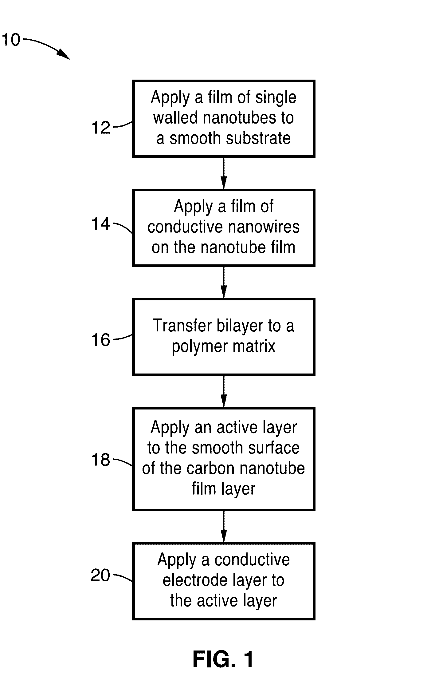
Examples
example 1
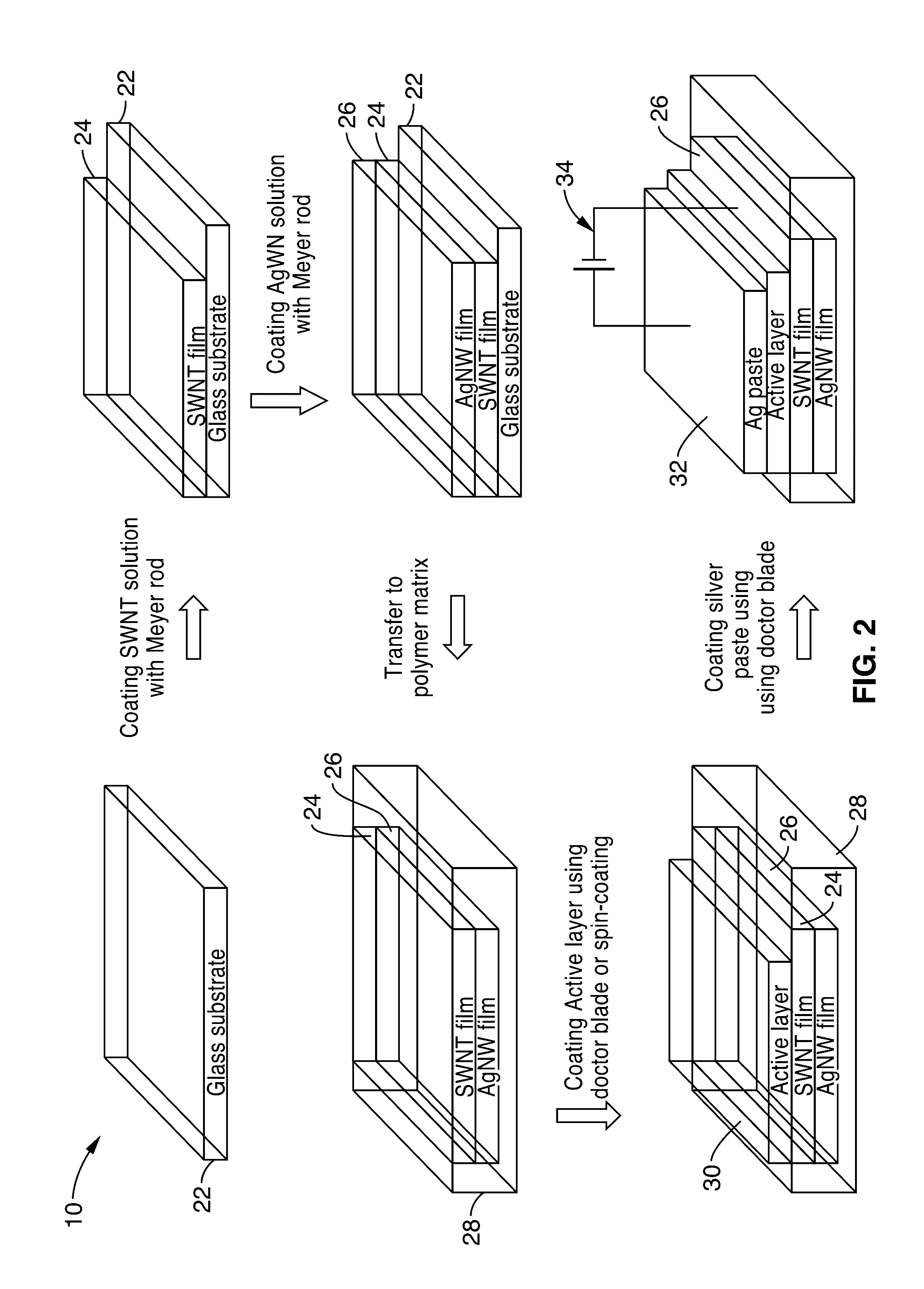
[0046]In order to demonstrate the functionality of the technology, LEC devices with one single walled carbon nanotube / Ag nanowires bilayer-polymer composite electrode were fabricated. Referring now to FIG. 2, a glass substrate 22 was provided and coated with a layer of single walled carbon nanotubes (SWCNT) 24 from a dispersion of nanotubes in isopropanol (IPA) and deionized water. In this procedure, 10 mg of functional SWCNTs were dispersed in 10 ml of a distilled water (DI-water) and isopropanol alcohol (IPA) mixture solution (volume ratio: DI-water / IPA=1 / 4) with the aid of sonication. The dispersion was subjected to centrifugation (at 8,000 rpm for 20 min) to remove undispersed SWCNT agglomerates and other large impurities. The resulting solution was then coated employing the Meyer rod on the glass release substrates to produce the SWCNT film 24.
[0047]The resulting carbon nanotube layer 24 was followed by a layer 26 of silver nanowires (AgNW)s from a dispersion of nanowires in IP...
example 2
[0057]The transmittance properties of the SWCNT films, bilayer films and the polymer composites were measured. A comparison of transmittance and sheet resistance performance for composite electrodes and ITO-glass electrode is tabulated in Table 1.
[0058]The transmittance spectra for the 10,000 ohm / sq SWCNT coating and various SWCNT / AgNW bilayer coatings on glass substrate were collected and evaluated. Although the SWCNT network is densely packed in stark contrast with that of the AgNW coating, the transmittance of the 10,000 Ω / sq SWCNT coating at 550 nm is around 89% (inclusive of glass substrate) and the 30Ω / sq sheet resistance had an 85% transmittance at 550 nm. When the sheet resistance of SWCNT coatings is lowered to 1.5 kΩ / sq in thicker coatings, the transmittance would diminish to only 76% at 550 nm. To lower to less than 100 Ohm / sq, the transmittance would be less than 60% at 550 nm, which is undesirable as a transparent electrode for PLECs.
[0059]The 10,000Ω / sq SWCNT coatings ...
example 3
[0062]The device structure and performance of LEO devices with ITO / glass, SWCNT-polymer composite, AgNW-polymer composite or SWCNT / AgNW bilayer-polymer composite electrode as anodes, and evaporated Al or Ag paste as cathodes were evaluated and tabulated in Table 2.
[0063]The commercial printing Ag paste has been used as the cathode in polymer LEDs. To investigate the performance of LEO devices using Ag paste as cathode, we first compared the two devices A and B of Table 2 using the same active layer (OC1C10:IC:LiTf) and anode (ITO / glass), but with evaporated Al (device A) and printing Ag paste (device B) as cathode respectively.
[0064]The current density-luminance-driving voltage characteristic curves (J-L-V) and current efficiency-luminance characteristic curves (η-L) of device A and device B, measured at a scanning voltage of 0.1 V / s, are presented with the corresponding maximum current efficiency, brightness, voltage and current density listed in Table 2.
[0065]The control device A ...
PUM
| Property | Measurement | Unit |
|---|---|---|
| surface height | aaaaa | aaaaa |
| sheet resistance | aaaaa | aaaaa |
| thickness | aaaaa | aaaaa |
Abstract
Description
Claims
Application Information
 - R&D
- Intellectual Property
- Life Sciences
- Materials
- Tech Scout
- Unparalleled Data Quality
- Higher Quality Content
- 60% Fewer Hallucinations
Browse by: Latest US Patents, China's latest patents, Technical Efficacy Thesaurus, Application Domain, Technology Topic, Popular Technical Reports.
© 2025 PatSnap. All rights reserved.Legal|Privacy policy|Modern Slavery Act Transparency Statement|Sitemap|About US| Contact US: help@patsnap.com