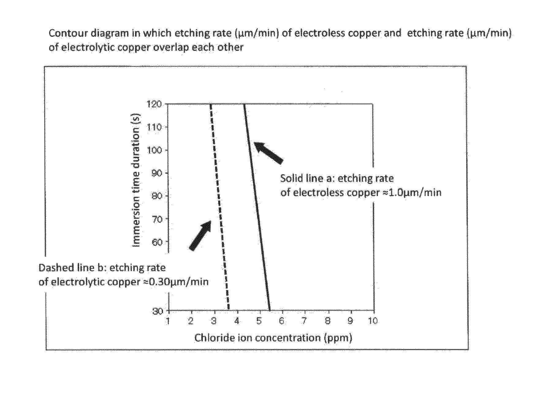
Method of treating wiring substrate and wiring substrate manufactured by the same
a technology of wiring substrate and wiring substrate, which is applied in the direction of conductive pattern formation, liquid/solution decomposition chemical coating, insulating substrate metal adhesion improvement, etc., can solve the problems of low etching rate, difficult control of side etching of copper used for wires, and high etching rate. , to achieve the effect of high density wiring and increased selection ratio
- Summary
- Abstract
- Description
- Claims
- Application Information
AI Technical Summary
Benefits of technology
Problems solved by technology
Method used
Image

Examples
first embodiment
[0044]The method of treating the wiring substrate in the first embodiment includes, in a semi-additive process:
[0045](1) contacting the wiring substrate with the pre-etching treatment liquid composition containing (a) a chloride ion and (b) a water, the wiring substrate containing a seed layer formed of an electroless copper and a wiring pattern formed of an electrolytic copper; and
[0046](2) continuously, etching the wiring substrate with the etching liquid composition containing (c) a hydrogen peroxide, (d) a sulfuric acid, (e) a tetrazole, (f) a chloride ion, (g) a copper ion and (h) a water.
[0047]In the first embodiment, the chloride ions are indispensable in the pre-etching treatment liquid composition (in the case where sulfuric acid is absent). Preferable compounds which generate chloride ions include hydrochloric acid, sodium chloride, potassium chloride, and ammonium chloride. Hydrochloric acid is especially preferable.
[0048]The chloride ions are contained in the pre-etching...
second embodiment
[0049]Also usable as a pre-etching treatment liquid composition is a composition in which a washing water containing sulfuric acid, used in a sulfuric acid washing step which is commonly performed before etching in order to remove an oxide layer from a surface of electrolytic copper, coexists with chloride ions.
[0050]A method of treating a wiring substrate in the second embodiment includes, in a semi-additive process:
[0051](1) contacting the wiring substrate with a pre-etching treatment liquid composition containing (i) a chloride ion, (j) a sulfuric acid and (k) a water, the wiring substrate containing a seed layer formed of an electroless copper and a wiring pattern formed of an electrolytic copper; and
[0052](2) continuously, etching the wiring substrate with an etching liquid composition containing (l) a hydrogen peroxide, (m) a sulfuric acid, (n) a tetrazole, (p) a chloride ion, (q) a copper ion and (r) a water.
[0053]Preferable compounds which generate chloride ions for the pre-...
example 3
Measurement Example 3
In the Case where the Treatment with the Pre-Etching Treatment Liquid Composition is Performed
[0138]A pre-etching treatment liquid composition (A3 liquid) and the etching liquid composition (B1 liquid) shown in Table 1 were prepared. The A3 liquid was prepared by adding 0.1 g of 0.0165% aqueous solution of sodium chloride (chloride ions: 0.1 ppm) to 99.9 g of 5% aqueous solution of sulfuric acid so that the total weight would be 100 g. The B1 liquid was prepared by mixing 2.33 g of 60% hydrogen peroxide solution, 9.13 g of 46% aqueous solution of sulfuric acid, 0.01 g of 1,5-dimethyltetrazole, 1.0 g of 0.0165% aqueous solution of sodium chloride and 9.82 g of copper sulfate pentahydrate, and adding ultrapure water for the remaining part so that the total amount would be 100 g. The content of each component shown in Table 1 is the ratio by mass of each component with respect to the total mass of the pre-etching treatment liquid composition or the etching liquid c...
PUM
| Property | Measurement | Unit |
|---|---|---|
| thickness | aaaaa | aaaaa |
| thickness | aaaaa | aaaaa |
| thickness | aaaaa | aaaaa |
Abstract
Description
Claims
Application Information
 - R&D
- Intellectual Property
- Life Sciences
- Materials
- Tech Scout
- Unparalleled Data Quality
- Higher Quality Content
- 60% Fewer Hallucinations
Browse by: Latest US Patents, China's latest patents, Technical Efficacy Thesaurus, Application Domain, Technology Topic, Popular Technical Reports.
© 2025 PatSnap. All rights reserved.Legal|Privacy policy|Modern Slavery Act Transparency Statement|Sitemap|About US| Contact US: help@patsnap.com