Reflective mask blank, reflective mask and method of manufacturing reflective mask
a reflective mask and blank technology, applied in the field of reflective mask blanks, reflective masks, and reflective mask manufacturing methods, can solve the problems of inability to obtain etching rates sufficient for forming transfer patterns, detrimental effects on the surface of absorber films, and inability to obtain transfer patterns. , to achieve the effect of favorable optical properties, favorable optical properties, and high transfer patterns
- Summary
- Abstract
- Description
- Claims
- Application Information
AI Technical Summary
Benefits of technology
Problems solved by technology
Method used
Image
Examples
example 1
[0178][Production of Reflective Mask Blank]
[0179]A substrate was prepared that was composed of SiO2—TiO2 glass having vertical and horizontal dimensions of about 152 mm×152 mm and having a thickness of about 6.25 mm. The edge faces and main surface of this substrate 1 were polished to a prescribed surface roughness (root mean square roughness Rq: not more than 0.15 nm), followed by carrying out prescribed washing treatment and drying treatment.
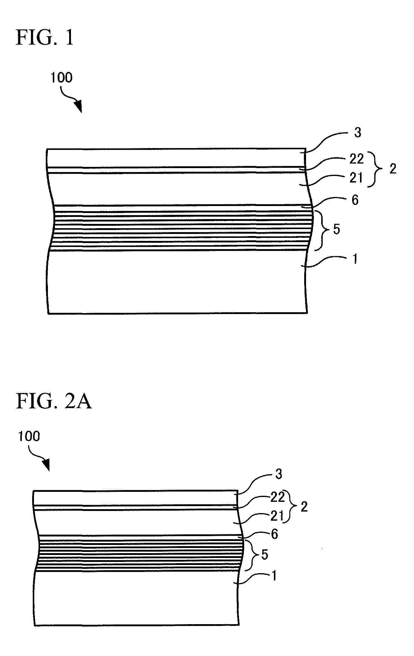
[0180]Next, the transparent substrate 1 was installed in an ion beam sputtering apparatus and the multilayer reflective film 5 was deposited by ion beam sputtering using a Si target and Mo target. More specifically, a 4.2 nm Si film was deposited after laminating 40 periods consisting of a 4.2 nm Si film and 2.8 nm Mo film. Continuing, the substrate 1 on which the multilayer reflective film 5 was formed was installed in a single-wafer DC sputtering apparatus, and the protective layer 6 composed of RuNb was formed to a thickness of 2.5 nm on th...
example 2
[0188][Production of Reflective Mask Blank]
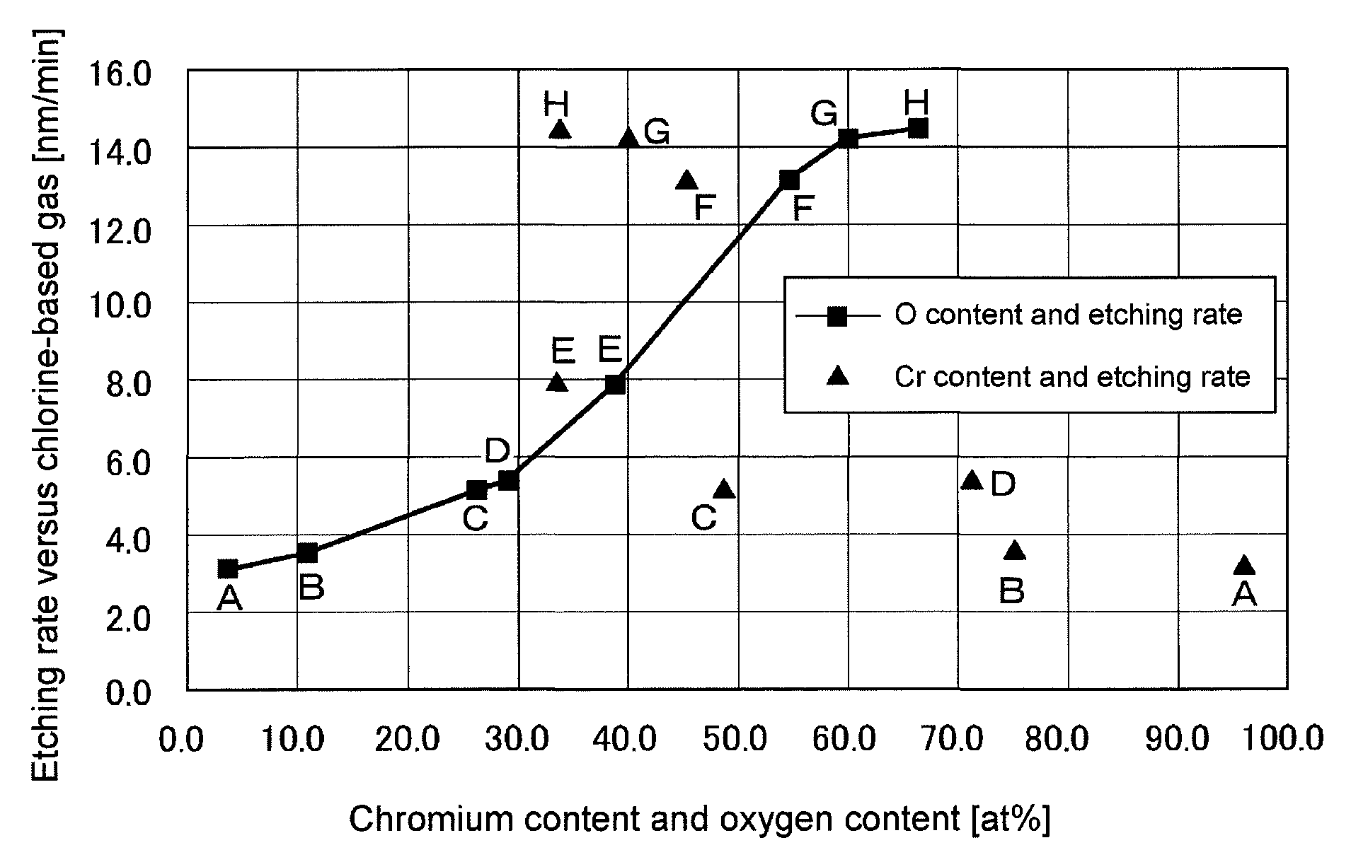
[0189]The reflective mask blank of Example 2 was fabricated according to the same procedure as Example 1 with the exception of changing the material of the etching mask film 3 to CrO (Cr: 46 at %, O: 54 at %) and changing the layer thickness to 6 nm.
[0190][Production of Reflective Mask]
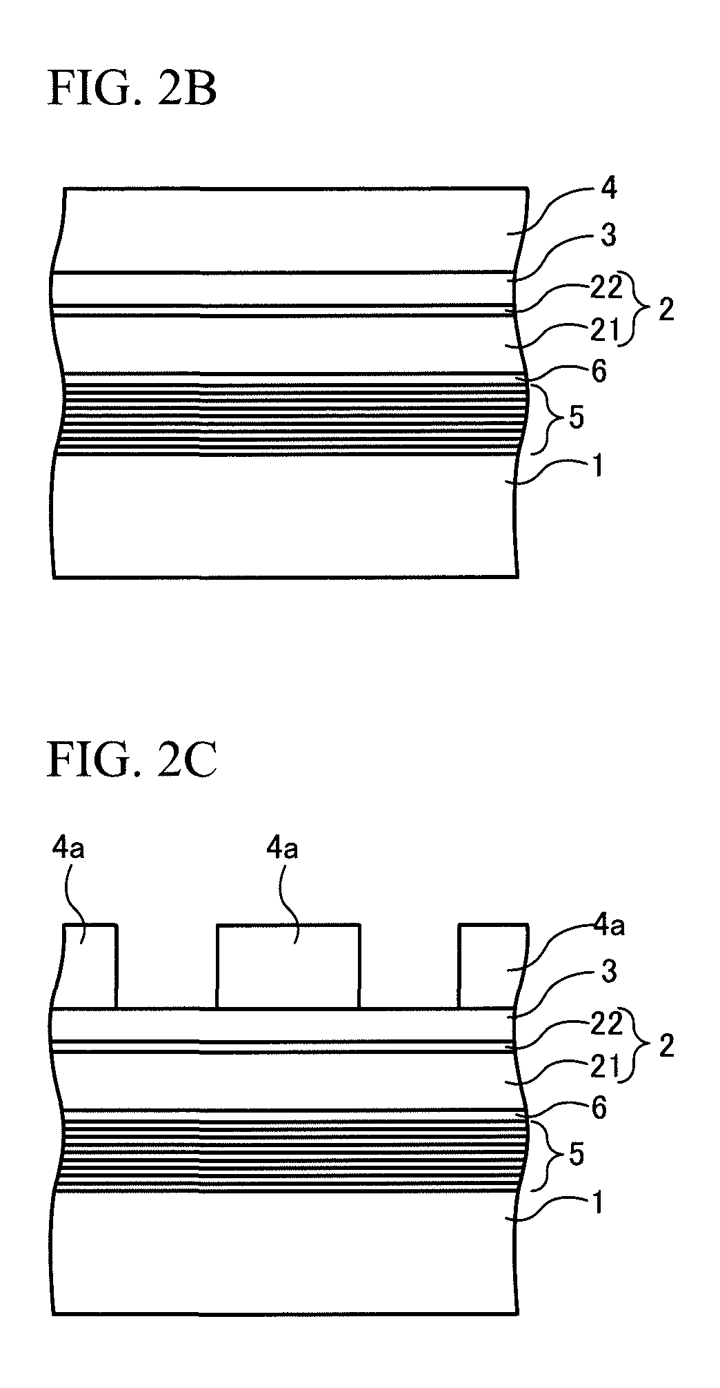
[0191]Next, the reflective mask 201 of Example 2 was fabricated according to the following procedure using the reflective mask blank 101 of Example 2. First, the resist film 4 composed of a chemically amplified resist for electron beam lithography was formed at a layer thickness of 60 nm on the etching mask film 3 by spin coating (see FIG. 4B). Next, the resist pattern 4a was formed in the resist film 4 by electron beam drawing followed by carrying out prescribed development treatment and washing treatment (see FIG. 4C). Furthermore, the transfer pattern formed by electron beam lithography had a 22 nm node fine pattern. Next, a transfer pattern (etching mask ...
example 3
[0193][Production of Reflective Mask Blank]
[0194]The reflective mask blank of Example 3 was fabricated according to the same procedure as Example 1 with the exception of carrying out the process for forming the highly oxidized layer 242 on the upper layer 24 of the absorber film 2 by ozone water treatment instead of hot water treatment. Ozone water treatment (surface treatment) was carried out by applying ozone-containing water having an ozone concentration of 50 ppm and temperature of 25° C. under the condition of a treatment time of 15 minutes.
[0195]The absorber film 2 was measured by Auger electron spectroscopy (AES) after the ozone water treatment. From the results, it was confirmed that the highly oxidized layer 242 was formed at a thickness of 2 nm on the surface layer of the upper layer 24. The oxygen content of this highly oxidized layer 242 was 71.4 at % to 67 at %. The compositions and optical properties of each of the other layers of the absorber film 2 were the same as t...
PUM
| Property | Measurement | Unit |
|---|---|---|
| binding energy | aaaaa | aaaaa |
| thickness | aaaaa | aaaaa |
| wavelength | aaaaa | aaaaa |
Abstract
Description
Claims
Application Information
 - R&D
- Intellectual Property
- Life Sciences
- Materials
- Tech Scout
- Unparalleled Data Quality
- Higher Quality Content
- 60% Fewer Hallucinations
Browse by: Latest US Patents, China's latest patents, Technical Efficacy Thesaurus, Application Domain, Technology Topic, Popular Technical Reports.
© 2025 PatSnap. All rights reserved.Legal|Privacy policy|Modern Slavery Act Transparency Statement|Sitemap|About US| Contact US: help@patsnap.com


