
Method for producing conducting and transparent films from combined graphene and conductive nano filaments

a technology of graphene and nano-fibre, which is applied in the direction of superimposed coating process, chemical coating, liquid/solution decomposition chemical coating, etc., can solve the problems of high sheet resistance, 10-50 ohms/, and are not suitable for the practical application of transparent cnt electrodes in current-based devices such as organic light-emitting diodes and solar cells. , to achieve the effect of reducing the resistance of the sheet, reducing the speed speed ratio ratio ratio ratio ratio ratio ratio ratio ratio ratio ratio ratio ratio ratio ratio ratio ratio ratio ratio ratio ratio ratio ratio ratio ratio ratio ratio ratio ratio ratio ratio ratio ratio ratio ratio ratio ratio ratio ratio ratio ratio ratio

Active Publication Date: 2014-10-28
GLOBAL GRAPHENE GRP INC
View PDF12 Cites 19 Cited by
  • Summary
  • Abstract
  • Description
  • Claims
  • Application Information

AI Technical Summary

Benefits of technology

The method results in a hybrid film with improved conductivity and transparency, comparable to high-end ITO glass, while being more cost-effective and suitable for flexible substrates, addressing the limitations of existing materials.

Problems solved by technology

However, there are several major issues associated with the use of CNTs for making a transparent conductive electrode (TCE).
The relatively high sheet resistance, compared with the approximately 10-50 ohms / square of high-end ITO on a plastic substrate, is far from being adequate for the practical application of transparent CNT electrodes in current-based devices, such as organic light emitting diodes and solar cells.
However, metal nanowires also suffer from the same problems as CNTs.
Additionally, although Ag nanowire films can show good optical and electrical performance, it has been difficult to make Ag nanowires into a free-standing thin film or a thin film of structural integrity coated on a substrate.
In particular, Ag nanowire films that are deposited on a plastic substrate exhibit unsatisfactory flexibility and mechanical stability in that the nanowires can easily come off.
Also, the surface smoothness is poor (surface roughness being too large).
Furthermore, all metal nanowires still have a long-term stability issue, making them unacceptable for practical use.
The intent was to protect the underlying Ag nanowire film, but this approach can introduce additional issues to the film, e.g. significantly reduced optical transmittance by carrying out multiple coating passes and increased sheet resistance (when the Ag nanowire film was coated with more than 3 passes).
Unfortunately, the interpenetrating network of graphite flakes and carbon nanotubes lead to a film that is only 80% transparent at 2 kOhms / square or 65% transparent at 1 kOhms / square (e.g., paragraph in both Ref. 9 and Ref. 11).
These values are absolutely unacceptable to the TCE industry.
Unfortunately, single-layer or few layer graphene films, albeit optically transparent, have a relatively high sheet resistance, typically 3×10²-105 Ohms / square (or 0.3-100 kΩ / □).
In other words, there is an inherent tradeoff between optical transparency and sheet resistance of graphene films: thicker films decrease not only the film sheet resistance but also the optical transparency.
However, the sheet resistance is still lower than desirable for certain applications.
However, the layer-by-layer procedure is not amenable to mass production of transparent conductive electrodes for practical uses.
Doping also adds an extra level of complexity to an already highly complex and challenging process that requires a tight vacuum or atmosphere control.
The CVD process and equipment are notoriously expensive.
These defects impede the flow of electrons and phonons.
A hybrid material containing both graphene oxide and CNT was formed into a thin film by Tung et al [Ref. 20], but the film does not exhibit a satisfactory balance of optical transparency and electrical conductivity.
The highest performance film shows optical transmittance of 92%, but this is achieved at an unacceptable sheet resistance of 636Ω / □.
The film with the lowest sheet resistance (240Ω / □ with un-doped RGO) shows 60% optical transmittance, which is not useful at all.
All these characteristics (defects and impurities) can significantly impede the transport of electrons and phonons in CVD graphene films.
Besides, CVD processes are slow and expensive.
As discussed above, the CNT mesh, metal nanowire mesh, CVD graphene film, GO film (including RGO film), CNT-graphite flake mesh, CNT-graphene oxide (GO) hybrid, and RGO-protected Ag nanowire mesh have been proposed to serve as a transparent and conductive electrode, but none has met the stringent combined requirements of transparency, conductivity, oxidation resistance or long-term stability, mechanical integrity and flexibility, surface quality, chemical purity, process ease, and low cost.
Surprisingly, this method inherently reduces contact resistance between metal nanowires (e.g. Ag or Cu nanowires) and that between a metal nanowire and a graphene material.

Method used


Image

  • Method for producing conducting and transparent films from combined graphene and conductive nano filaments
  • Method for producing conducting and transparent films from combined graphene and conductive nano filaments
  • Method for producing conducting and transparent films from combined graphene and conductive nano filaments

Examples


example 1

Direct Ultrasonication Production of Pristine Graphene from Natural Graphite in a Low Surface Tension Medium

[0095]As an example, five grams of natural graphite, ground to approximately 20 μm or less in sizes, were dispersed in 1,000 mL of n-Heptane to form a graphite suspension. An ultrasonicator tip was then immersed in the suspension, which was maintained at a temperature of 0-5° C. during subsequent ultrasonication. An ultrasonic energy level of 200 W (Branson S450 Ultrasonicator) was used for exfoliation and separation of graphene planes from dispersed graphite particles for a period of 1.5 hours. The average thickness of the resulting pristine graphene sheets was 1.1 nm, having mostly single-layer graphene and some few-layer graphene.

example 2

Preparation of Pristine Graphene from Natural Graphite in Water-Surfactant Medium Using Direct Ultrasonication

[0096]As another example, five grams of graphite flakes, ground to approximately 20 μm or less in sizes, were dispersed in 1,000 mL of deionized water (containing 0.15% by weight of a dispersing agent, Zonyl® FSO from DuPont) to obtain a suspension. An ultrasonic energy level of 175 W (Branson S450 Ultrasonicator) was used for exfoliation, separation, and size reduction for a period of 1.5 hour. This procedure was repeated several times, each time with five grams of starting graphite powder, to produce a sufficient quantity of pristine graphene for thin film deposition.

example 3

Preparation of Pristine Graphene Using Supercritical Fluids

[0097]A natural graphite sample (approximately 5 grams) was placed in a 100 milliliter high-pressure vessel. The vessel was equipped with security clamps and rings that enable isolation of the vessel interior from the atmosphere. The vessel was in fluid communication with high-pressure carbon dioxide by way of piping means and limited by valves. A heating jacket was disposed around the vessel to achieve and maintain the critical temperature of carbon dioxide.

[0098]High-pressure carbon dioxide was introduced into the vessel and maintained at approximately 1,100 psig (7.58 MPa). Subsequently, the vessel was heated to about 70° C. at which the supercritical conditions of carbon dioxide were achieved and maintained for about 3 hours, allowing carbon dioxide to diffuse into inter-graphene spaces. Then, the vessel was immediately depressurized “catastrophically’ at a rate of about 3 milliliters per second. This was accomplished by...


PUM

PropertyMeasurementUnit
sheet resistanceaaaaaaaaaa
impingement speedaaaaaaaaaa

Abstract

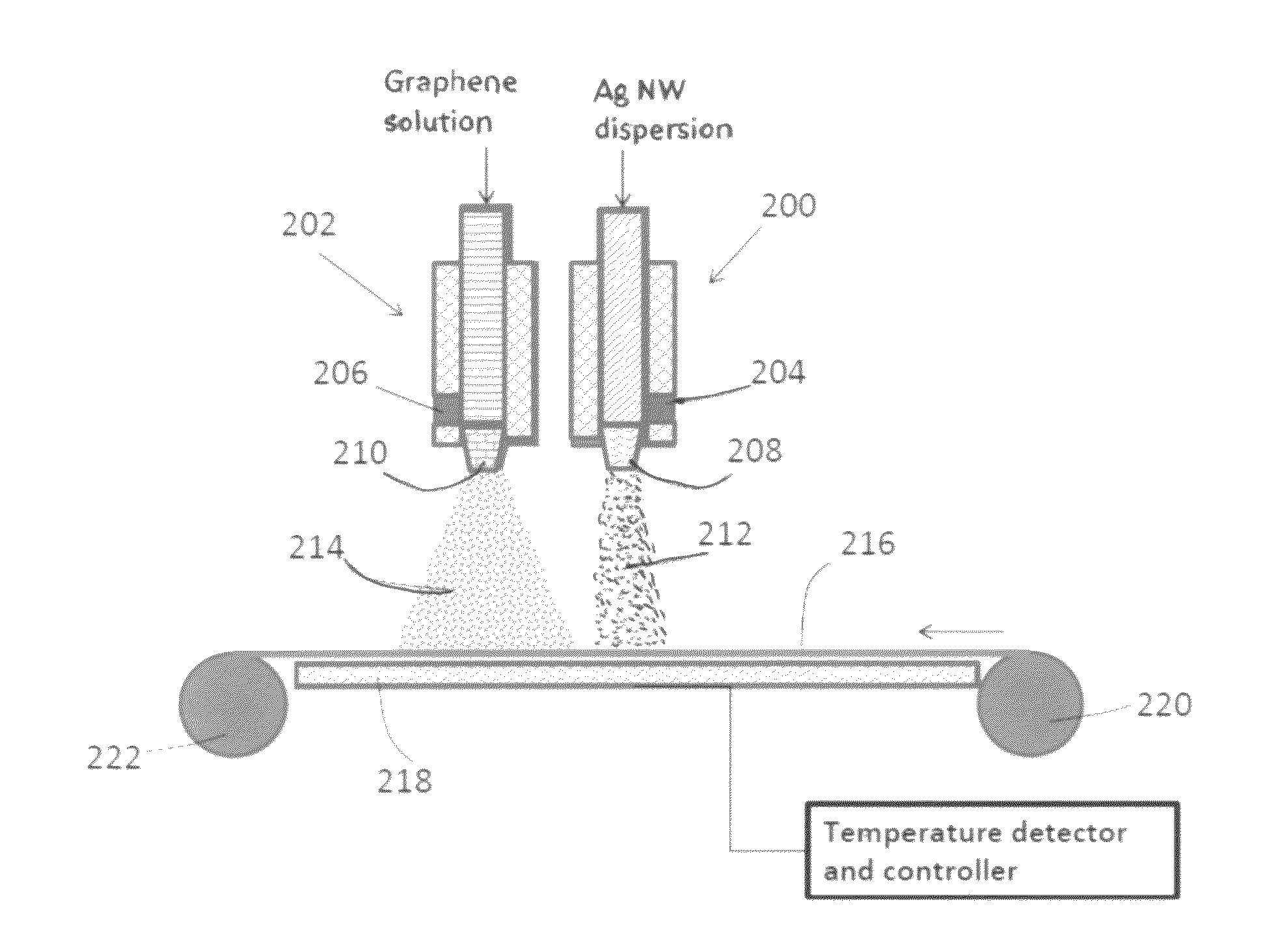
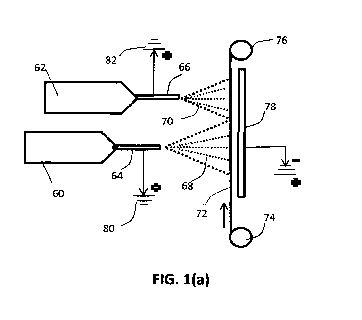
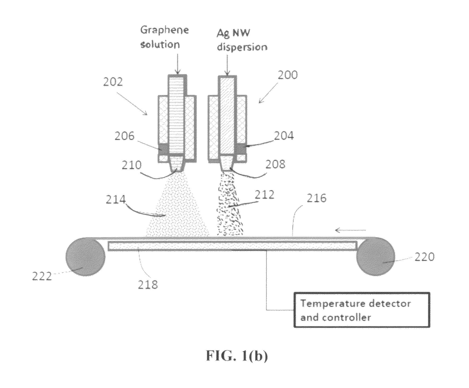
A method of producing a transparent and conductive film, comprising (a) forming aerosol droplets of a first dispersion comprising a first conducting nano filaments in a first liquid; (b) forming aerosol droplets of a second dispersion comprising a graphene material in a second liquid; (c) depositing the aerosol droplets of a first dispersion and the aerosol droplets of a second dispersion onto a supporting substrate; and (d) removing the first liquid and the second liquid from the droplets to form the film, which is composed of the first conducting nano filaments and the graphene material having a nano filament-to-graphene weight ratio of from 1 / 99 to 99 / 1, wherein the film exhibits an optical transparence no less than 80% and sheet resistance no higher than 300 ohm / square.

Description

[0001]This application claims the benefits of the following patent applications: Yi-jun Lin, Aruna Zhamu, and Bor Z. Jang, “Highly Conducting and Transparent Film and Process for Producing Same,” U.S. patent application Ser. No. 13 / 815,316 (Feb. 21, 2013). Yi-jun Lin, Aruna Zhamu, and Bor Z. Jang, “Process for Producing Highly Conducting and Transparent Films from Graphene Oxide-Metal Nanowire Hybrid Materials,” U.S. patent application Ser. No. 13 / 815,317 (Feb. 21, 2013).FIELD OF THE INVENTION[0002]The present invention relates generally to the field of transparent conductive electrodes for solar cell, photo-detector, light-emitting diode, touch screen, and display device applications and, more particularly, to a graphene / nano filament-based hybrid film with a combination of exceptional optical transparency and high electrical conductivity (or low sheet resistance).BACKGROUND OF THE INVENTION[0003]The following references are related to the art of “transparent and conductive electro...

Claims


Application Information

Patent Timeline
Patent Type & Authority Patents(United States)
IPC IPC(8): C23C16/26B05D1/02B05D5/12C23C18/00B05D7/12H01B13/00
CPCB05D5/12B05D1/02H01B13/0036H01L31/1884B05D7/12Y10S427/101C23C16/26B22F1/0025B22F7/04B22F2007/042C22C26/00H01L51/0021H01L51/0048H01L51/444B22F1/0547H10K71/60H10K85/221H10K30/821Y02E10/50
Inventor ZHAMU, ARUNALIN, YI-JUNJANG, BOR Z.
Owner GLOBAL GRAPHENE GRP INC
Learn More