
Patterning process

a pattern and pattern technology, applied in the field of pattern pattern formation process, can solve the problems of low resist etching resistance, low etching resistance of scanner, abandonment of development of this technology, etc., and achieve the effect of improving the resolution of fine trench or hole pattern, high dry etching resistance, and high dissolution contrast in organic solvent developmen

Active Publication Date: 2014-05-13
SHIN ETSU CHEM IND CO LTD
View PDF34 Cites 3 Cited by
  • Summary
  • Abstract
  • Description
  • Claims
  • Application Information

AI Technical Summary

Benefits of technology

The patent describes a special resist composition that has good resistance to dissolution in organic solvents and high dry etching resistance. This composition is especially useful for making fine patterns in semiconductor devices. When a negative pattern is created using this resist, the resulting pattern has improved resolution and high resistance to dry etching.

Problems solved by technology

However, for the reasons that the projection lens uses a large amount of expensive CaF2 single crystal, the scanner thus becomes expensive, hard pellicles are introduced due to the extremely low durability of soft pellicles, the optical system must be accordingly altered, and the etch resistance of resist is low; the development of F2 lithography was abandoned and instead, the ArF immersion lithography was introduced.
The development of this technology was abandoned because LUAG, a high refractive index lens candidate had a low transmittance and the refractive index of liquid did not reach the goal of 1.8.
As compared with the line pattern, the hole pattern is difficult to reduce the feature size.
This, however, results in the exposure margin being extremely narrowed.
With the hole shrinking method, the hole size can be shrunk, but the pitch cannot be narrowed.
Although a hole pattern can be formed at a wide margin by combining X and Y lines and using dipole illumination featuring a high contrast, it is difficult to etch vertically staged line patterns at a high dimensional accuracy.
The methacrylate resins, however, have the drawback that the resin backbone is short of dry etch resistance.
When the substrate is etched using the resist film as a mask, there is a likelihood of pattern transfer failure.
However, the polymer is not regarded sufficient with respect to the resolution and roughness of a fine pattern necessary for the fabrication of advanced microelectronic devices.
Increasing the proportion of acid labile group introduced is effective for enhancing the dissolution contrast and improving the resolution, but in the case of negative development, may worsen dry etch resistance for the above-described reason.

Method used


Image

  • Patterning process
  • Patterning process
  • Patterning process

Examples


example

[0162]Examples of the invention are given below by way of illustration and not by way of limitation. The abbreviation “pbw” is parts by weight. For all polymers, Mw and Mn are determined by GPC versus polystyrene standards using tetrahydrofuran solvent.

Preparation of Resist Composition

[0163]A resist solution was prepared by dissolving components in a solvent in accordance with the recipe shown in Table 1, and filtering through a Teflon® filter with a pore size of 0.2 μm. The polymers as base resin in Table 1 have a structure, molecular weight (Mw) and dispersity (Mw / Mn) as shown in Tables 2 to 5. In Tables 2 to 5, the value in parentheses indicates a constitutional ratio (mol %) of the relevant recurring unit. The structure of photoacid generators in Table 1 is shown in Table 5. The structure of quenchers in Table 1 is shown in Table 6.

[0164]It is noted that in Table 1, Resists 1 to 18 correspond to resist compositions used in the inventive process and Resists 19 to 24 are comparati...


PUM

PropertyMeasurementUnit
wavelengthaaaaaaaaaa
transmittanceaaaaaaaaaa

Abstract

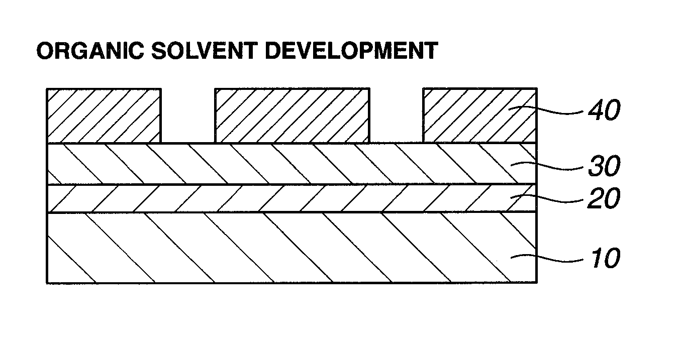
A negative pattern is formed by applying a resist composition onto a substrate, baking, exposing to high-energy radiation, baking (PEB), and developing the exposed resist film in an organic solvent developer to selectively dissolve the unexposed region of resist film. The resist composition comprising a hydrogenated ROMP polymer comprising recurring units having an acid labile group-protected carboxyl group and recurring units having a lactone structure displays a high dissolution contrast in organic solvent development, and exhibits high dry etch resistance even when the acid labile group is deprotected through exposure and PEB.

Description

CROSS-REFERENCE TO RELATED APPLICATION[0001]This non-provisional application claims priority under 35 U.S.C. §119(a) on patent application No. 2011-096119 filed in Japan on Apr. 22, 2011, the entire contents of which are hereby incorporated by reference.TECHNICAL FIELD[0002]This invention relates to a pattern forming process and more particularly, to a negative pattern forming process including forming a resist film from a specific resist composition, exposure, post-exposure baking to effect deprotection reaction under the catalysis of an acid generated by a photoacid generator, and developing with an organic solvent to dissolve the unexposed region, but not the exposed region of the resist film.BACKGROUND ART[0003]In the recent drive for higher integration densities and operating speeds in LSI devices, the pattern rule is made drastically finer. The photolithography which is currently on widespread use in the art is approaching the essential limit of resolution determined by the wa...

Claims


Application Information

Patent Timeline
Patent Type & Authority Patents(United States)
IPC IPC(8): G03F7/26
CPCG03F7/325G03F7/0397G03F7/2041G03F7/203G03F7/0395G03F7/00G03F7/004G03F7/26G03F7/30G03F7/32
Inventor KOBAYASHI, TOMOHIROKINSHO, TAKESHISEKI, AKIHIROKUMAKI, KENTARO
Owner SHIN ETSU CHEM IND CO LTD
Learn More