Process for producing silicon oxide thin film or silicon oxynitride compound thin film and thin film obtained by the process
a technology of silicon oxide and compound, which is applied in the direction of electrical equipment, basic electric elements, solid-state devices, etc., can solve the problems of difficult to obtain the flexibility expected material, the protective film manufactured by the manufacturing method using the solution process does not fully perform the functions, and the surrounding is sensitive, etc., to achieve high strength, high barrier properties, and efficient manufacturing
- Summary
- Abstract
- Description
- Claims
- Application Information
AI Technical Summary
Benefits of technology
Problems solved by technology
Method used
Image
Examples
example 1
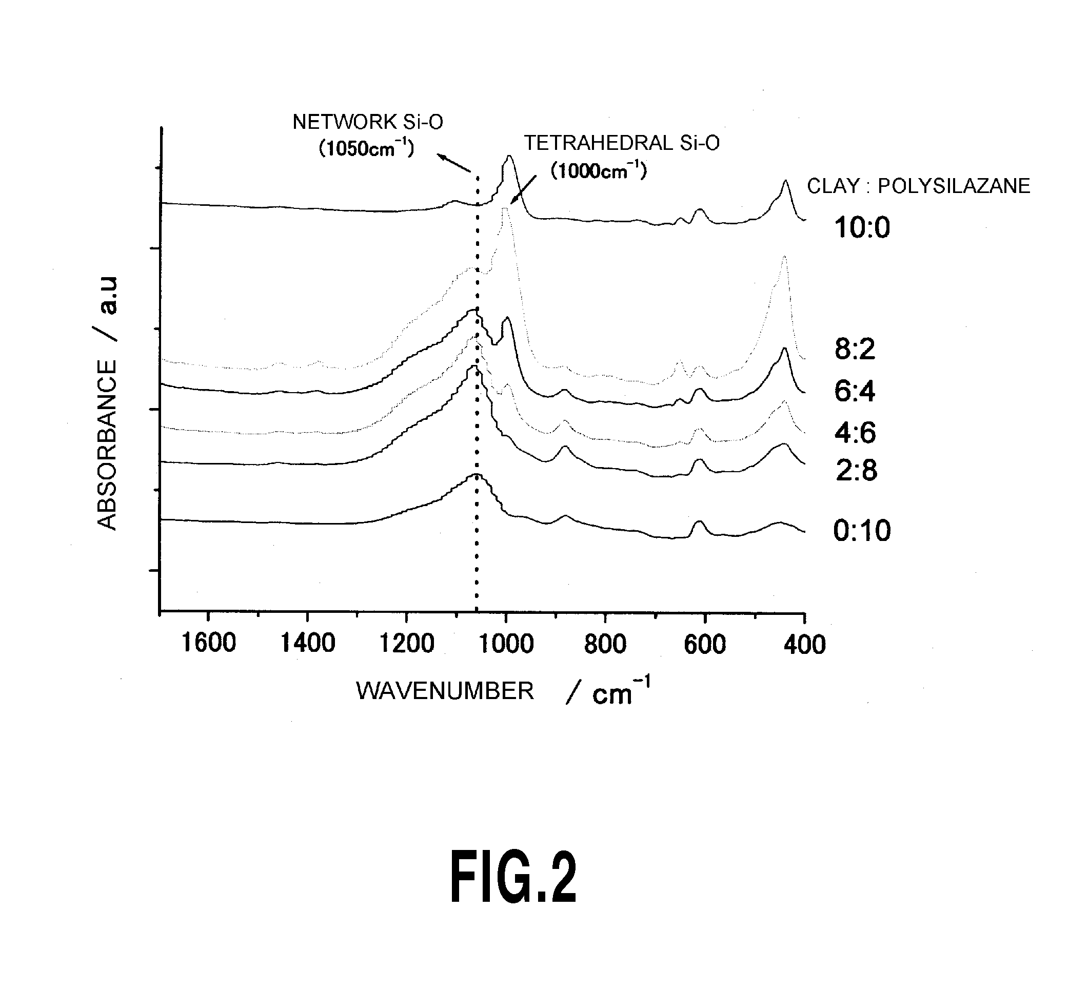
[0070]An n-type silicon wafer was subjected to ultrasonic cleaning for 15 minutes by using a neutral detergent (PURESOFT, manufactured by AS ONE Corporation) diluted with pure water to 5 fold, followed by ultrasonic cleaning in pure water for 15 minutes, to remove impurities. In addition, an UV-Ozone cleaner was applied to conduct ultraviolet radiation irradiation cleaning in an oxygen atmosphere for 20 minutes. The substrate thus cleaned was coated with a solution by spin-coating at 2000 rpm at 80° C. for drying 1 hour, the solution being prepared by mixing a dichloroethane solution of 5% by weight of LUCENTITE SPN (manufactured by CO-OP Chemical Co., Ltd.) and a specified amount of 20% by weight of polysilazane NP110 (manufactured by AZ Electronic Materials Limited) so that the weight ratio therebetween becomes 0:10, 2:8, 4:6, 6:4, 8:2, and 10:0, respectively, after film forming. Subsequently, the film was dried in a vacuum chamber at 100° C. for 30 minutes, followed by ultraviole...
example 2
[0074]On a PET substrate having a thickness of 50 μm, there was formed a film by using the blade coating method to coat a solution, followed by drying at 80° C. for 1 hour, the solution being prepared by mixing a dichloroethane solution of 5% by weight of LUCENTITE SPN (manufactured by CO-OP Chemical Co., Ltd.) and a specified amount of 20% by weight of polysilazane NP110 (manufactured by AZ Electronic Materials Limited) so that the weight ratio therebetween becomes 0:10, 2:8, 4:6, 6:4, 8:2, and 10:0, respectively, after film forming. After the coating, the film was dried in a vacuum chamber at 100° C. for 30 minutes, followed by irradiation with an ultraviolet radiation having a wavelength of 172 nm for 10 minutes in a stream of gas mixture of oxygen and nitrogen.
[0075]For the films thus formed, the effect of the clay addition on the barrier properties against water vapor was evaluated by the cup method (JIS Z0208). The results are shown in FIG. 6. In order to perform evaluation wi...
example 3
[0076]When the protective film is coated only on a specified position, use of printing method such as screen printing, gravure printing, flexographic printing, relief printing, intaglio printing, and offset printing; ink-jet printing; dispenser printing; drop-cast printing; or the like is conceived. The viscosity of the solution is required to be adjusted to the value suitable to the method. Generally the viscosity of the solution is required to be arbitrarily adjustable within a range of 0.05 to 100 Pa·s. An optimum viscosity is considered to be in a range of 10 to 100 Pas for the relief printing, 0.1 to 0.2 Pa·s for the flexographic printing, 0.05 to 0.2 Pa·s for the gravure printing, 100 Pa·s for the offset printing, and 1 to 10 Pa·s for the screen printing.
[0077]Table 1 shows the viscosity when the concentration ratio of dichloroethane solution of LUCENTITE SPN (manufactured by CO-OP Chemical Co., Ltd.) to polysilazane NP110 (manufactured by AZ Electronic Materials Limited) vari...
PUM
| Property | Measurement | Unit |
|---|---|---|
| thickness | aaaaa | aaaaa |
| wavelength | aaaaa | aaaaa |
| thickness | aaaaa | aaaaa |
Abstract
Description
Claims
Application Information
 - R&D
- Intellectual Property
- Life Sciences
- Materials
- Tech Scout
- Unparalleled Data Quality
- Higher Quality Content
- 60% Fewer Hallucinations
Browse by: Latest US Patents, China's latest patents, Technical Efficacy Thesaurus, Application Domain, Technology Topic, Popular Technical Reports.
© 2025 PatSnap. All rights reserved.Legal|Privacy policy|Modern Slavery Act Transparency Statement|Sitemap|About US| Contact US: help@patsnap.com


