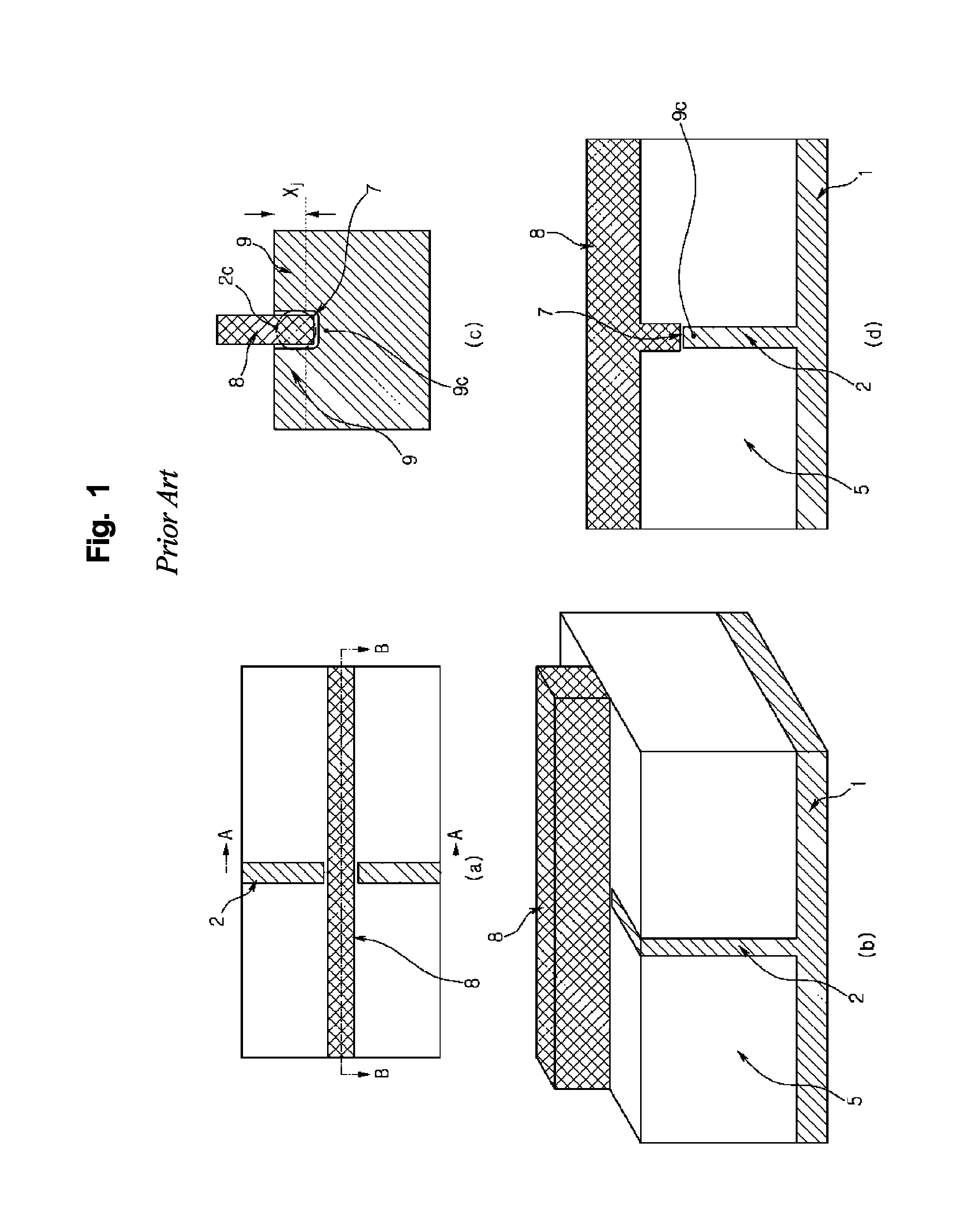
Saddle type MOS device
a mos device and saddle technology, applied in the direction of mos devices, basic electric elements, electrical equipment, etc., can solve the problems of serious back bias effect, large increase in threshold voltage of nmos devices for negative () back bias, etc., to reduce the change in threshold voltage, improve the control of the channel, and reduce the effect of the change of threshold voltag
- Summary
- Abstract
- Description
- Claims
- Application Information
AI Technical Summary
Benefits of technology
Problems solved by technology
Method used
Image

Examples
Embodiment Construction
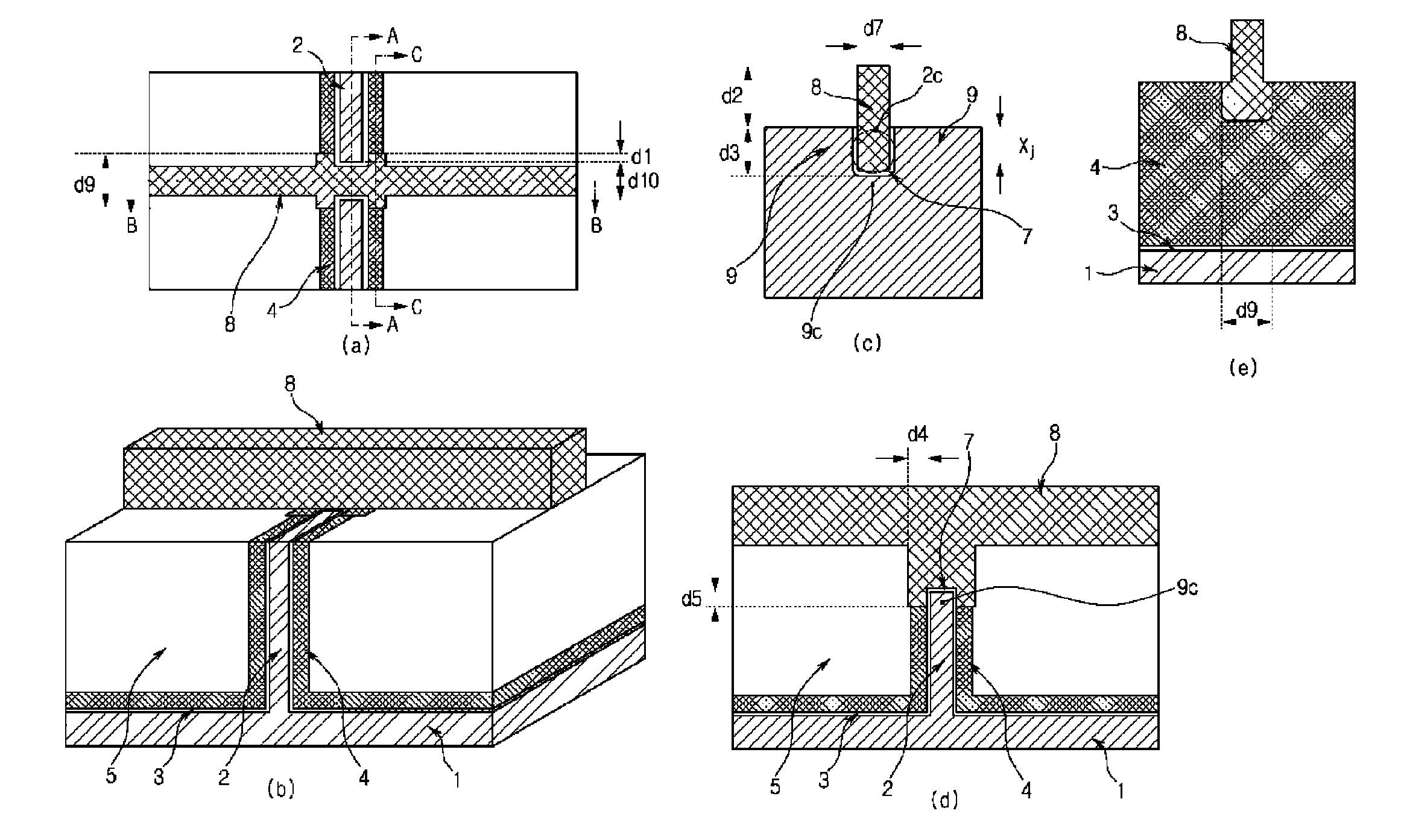
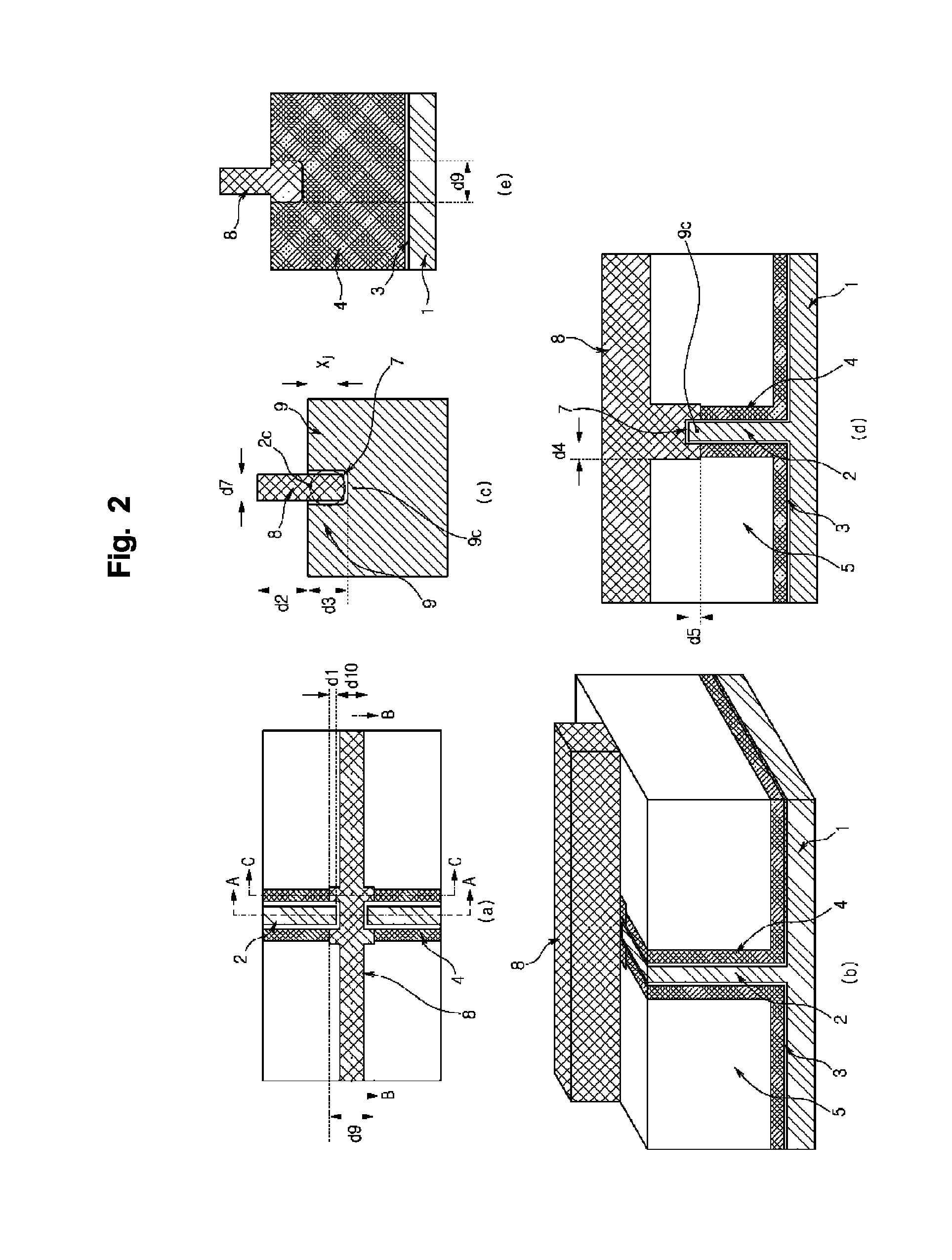
[0030]The present invention provides a nano-scale MOS device having a recessed channel and a saddle-type gate structure. In other words, the recessed channel region and the gate electrode are formed in the form of a saddle. The inventive MOS device is mainly characterized in that a channel region is recessed, a gate insulating film and a gate electrode are formed on the surface of the recess region of the recessed channel and sides of the recessed channel near the recess region thereof, and the gate electrode is self-aligned with the recessed channel.
[0031]More specifically, the present invention provides a MOS device comprising: a silicon substrate 1 having formed thereon a wall-type silicon body 2 connected with the substrate; a first insulating film 3 formed on the surface of the silicon substrate 1 and the surface of the silicon body 2; a nitride film 4 formed on the first insulating film 3; a second insulating film 5 for element isolation formed on the nitride film 4; a region ...
PUM
 Abstract
Description
Claims
Application Information
 - R&D
- Intellectual Property
- Life Sciences
- Materials
- Tech Scout
- Unparalleled Data Quality
- Higher Quality Content
- 60% Fewer Hallucinations
Browse by: Latest US Patents, China's latest patents, Technical Efficacy Thesaurus, Application Domain, Technology Topic, Popular Technical Reports.
© 2025 PatSnap. All rights reserved.Legal|Privacy policy|Modern Slavery Act Transparency Statement|Sitemap|About US| Contact US: help@patsnap.com